The register transfer level (RTL) is another design abstraction level that represents digital circuits at a higher level than previous abstractions. This once again improves readability of diagrams and schematics. The register transfer level focuses on digital circuits and their flows of binary signals (data) between registers, and the logical operations performed on those signals. Registers are functional units that contain some fast storage, and it will be explained later how they work. Therefore, the register transfer level primarily consists of functional units that either store data, or process them in a certain way, and communication channels that interconnect these functional units.
In digital integrated circuits, numerous functional units perform logical operations at the same time. In cases where functional units rely on input signals from previous components, they can only start processing when these previous components have completely finished their logic operations. As a subsequent functional unit has no information on the processing status of its previous components, almost all functional units must be synchronized by reliable external impulses. These external impulses are provided by a clock signal that oscillates between a high (1) and a low (0) voltage. A typical clock signal uses a square wave with a constant frequency. The clock signal is supplied to those functional units that require synchronization. Depending on the design of those units, these can become active at the rising edge of the clock signal, at the falling edge of the clock cycle, or during the intervals where the clock signal is high or low. The figure below shows a schematic representation of a clock signal.
A cycle refers to a single complete traversal of the signal: From the rising edge, through the phase where the voltage of the clock signal is high, over the falling edge, through the phase where the voltage of the clock signal is zero, until the start of the next cycle. The cycle time refers to the time the clock signal needs to traverse one complete cycle. The cycle time is chosen so that the slowest functional unit still has enough time to complete its operation. In today’s computer processors, cycle times are within the range of nanoseconds (billionth of a second). The clock frequency (also referred to as clock rate or clock speed) is the number of cycles the clock performs in one second. Therefore, in order to get the frequency, one second must be divided by the cycle time. With a cycle time of one nanosecond, the correspondent clock frequency is one gigahertz (GHz). Clock signals are produced by clock generator circuits. These usually rely on a crystal resonator that is combined with an amplifier circuit. Most integrated circuits require an external clock generator to provide the clock signal.

Any functional unit consists of logic networks that are implemented from logic gates. A distinction is made between combinational logic functions and sequential logic functions.
In a combinational circuit, the output is only determined by the logical function of their present input states (logic 0 or logic 1). As soon as the input changes, all information about the previous inputs is lost, and the output is re-calculated. For that reason, combinational logic circuits have no memory. Combinational circuits are also known as time-independent and stateless circuits. Combinational logic is very commonly used in arithmetic logic units using digital adders or other circuits.
The following diagram summarizes both types of logic functions:
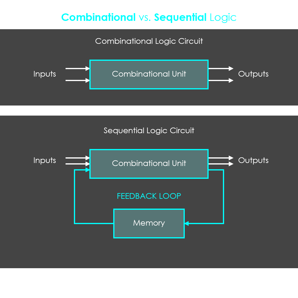
In a sequential circuit, the output is dependent on both the present input states and the previous output state. For that reason, sequential logic circuits have some form of memory built in. This is achieved by a feedback loop that connects the output back to the input. Sequential logic is most commonly used in registers.
Here are some chapters about combinational functional units, and what circuits are used to implement them.
Here are some chapters about sequential functional units, and what circuits are used to implement them.
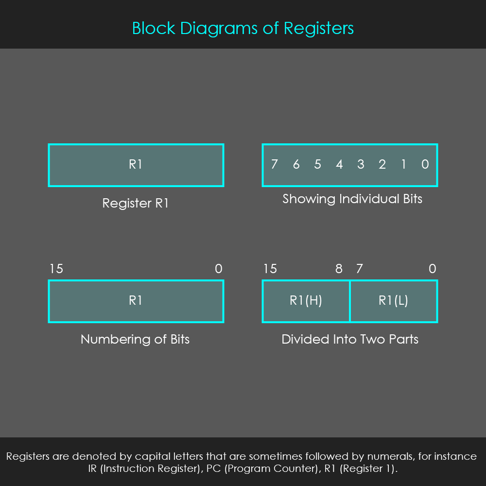
In computer science, register transfer language is a type of intermediate representation that is very close to assembly language. It is a notation that is used to describe data transfers between registers. Registers are typically denoted by capital letters and (sometimes) numerals, for instance IR (Instruction Register), PC (Program Counter), R1 (Register 1). Individual bits can be indicated by placing them in parentheses: IR(0-7), R2(4). In schematics of integrated circuits, registers can be represented by different types of block diagrams as shown in the illustration.
A simple rectangle indicates a register. Top left: Note that this register shows no information about the number of bits it contains. In integrated circuits where all registers operate on the same number of bits, it is sufficient to have this very basic type of register diagram. Top right: This diagram is showing the individual bits the register contains. Lower left: This diagram contains the name of the register as well as the bit width. Lower right: A 16-bit register R1 is divided into two parts. R1(L) refers to the lower byte (0-7) of the 16-bit register whereas R1(H) refers to the higher byte (8-15) of the 16-bit register.
In order to transfer information between registers, there are various instruction statements. The diagram shows some of these register transfer language instructions.
The statement R2 ← R1 denotes a transfer of the content of register R1 into register R2. With this operation, the content of the destination register R2 is replaced with the content of R1. By contrast, the content of the source register R1 does not change after the transfer. The statement R2 ← R1, R7 ← R6 denotes two simultaneous transfers of information. In practice, it is required that register transfers only take place under certain conditions, for instance when a certain control signal is high. The statement P: R2 ← R1 denotes a conditional transfer. This means that the content of R2 is replaced with the content of R1 only when the condition P = 1 is given. Such a conditional transfer is typically implemented by a control line that activates the parallel load function of the destination register, and P refers to the signal status of that control line.
This diagram summarizes the most common symbols for register transfers that allow some more detailed instructions.
Any statement that specifies a register transfer implies that connections between the outputs of the source register and the inputs of the destination register are available, as well as control hardware to implement the microoperation. Also, it is required that the destination register has a parallel load capability. The diagram shows a basic configuration of two registers that can perform a simple register transfer operation once the control signal P is high.
Microoperations are divided into four different categories:
1] Register transfer microoperations transfer data from one register to another register.
2] Arithmetic microoperations perform operations like addition, subtraction, incrementation, decrementation on data in registers.
3] Logic microoperations perform binary operations (AND, OR, XOR) on data. For instance, an exclusive-OR (XOR) microoperation on the contents of two registers (R1: 1100, R2: 1010) results in the new 4-bit string 0110.
4] Shift microoperations perform shifts on data in registers.
If more than one source register exists, binary information can be transferred via a communication system called the bus. There are different types of bus systems depending on the data that they transfer (address bus, data bus, control bus), but they are all based on the same principles. Further details on bus systems can be found here: