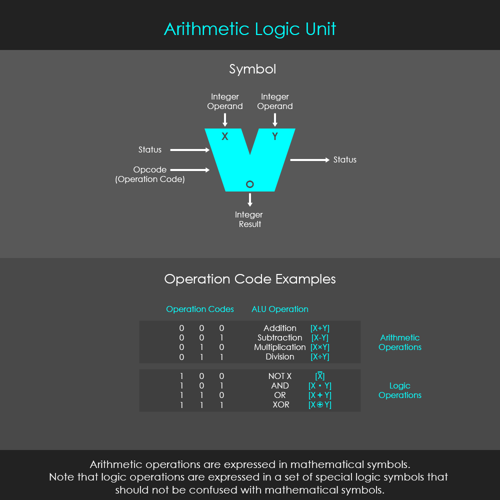
Probably the most common use of combinational logic is in the arithmetic logic unit. An arithmetic logic unit (ALU) is a functional unit that performs arithmetic (addition, subtraction, etc.) and logical (AND, OR, etc.) operations on integer binary numbers. It is also one of the most fundamental units of many computing circuits, including the central processing unit (CPU) of computers, and the graphic processing unit (GPU) of video cards. Individual ALUs can be highly specialized to certain logic operations, and an integrated circuit may include multiple ALUs.
An ALU has various inputs and various outputs. Inputs of an ALU are primarily the operands which are the data to be operated on. In addition, an ALU has opcodes (operation codes) as inputs to control the type of operation the ALU shall perform. A separate status input typically contains information about a previous operation. The output of an ALU is the result of the performed operation. In many designs, the ALU also has a status output that is either forwarded to other components of the ALU for further processing, or used as a status flag that indicates different conditions of an operation. For instance, if an ALU compares two numbers, a status flag can indicate whether both numbers are equal or unequal.
The diagram includes a small example of operations an ALU can perform. Some other very typical opcodes are ‘compare’, ‘increment’, ‘decrement’, ‘shift right’, ‘shift left’, ‘pass through’, and modulo function (an operation performed to check whether a number is even or odd). Modern ALUs feature more than 100 instruction opcodes.
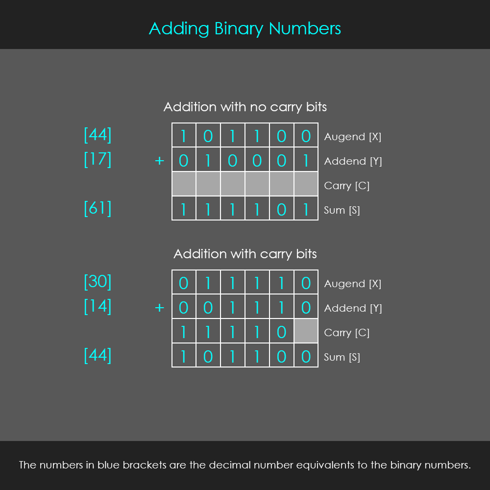
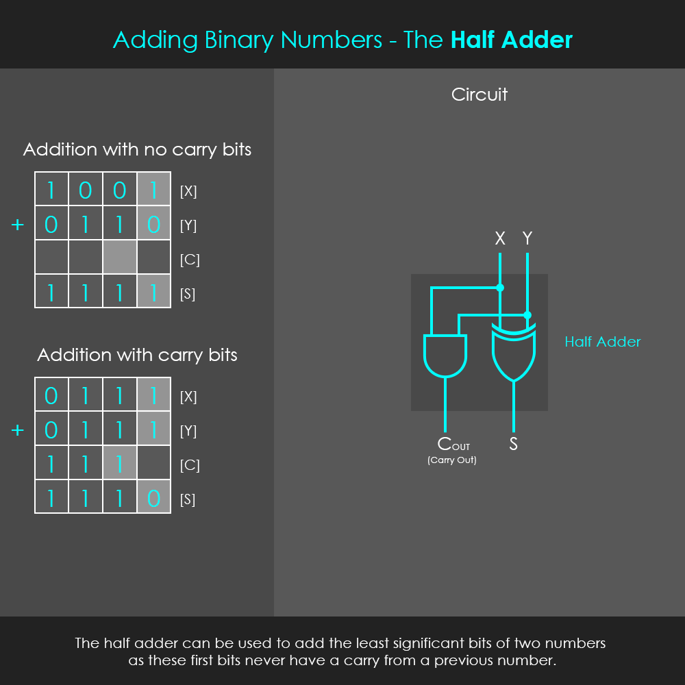
Adding two binary numbers is done by aligning the numbers vertically from the least significant bit. If one bit number is shorter than the other, the shorter number is padded with leading zeros. Each bit position from one number is added to the same bit position of the other number, starting from the right and proceeding to the left. In principle, the addition is identical to an addition in the decimal system, the only difference is that ‘2’ must already be represented as a binary ’10’. So 0+0=0, 0+1=1, and 1+0=1. In case 1+1 are added, the sum is a binary 10, so the output for the least significant bit of the sum is 0 and a 1 is carried over one position to the left for further addition.
The circuit that can perform the addition for the least significant bits of two binary numbers is called a half adder. This type of circuit consists of an XOR gate and an AND gate connected in parallel. The diagram shows the layout of a half adder circuit.
The XOR produces the sum, and the AND gate produces the carry out signal. So looking at the possible calculations again, for 0+0, neither the XOR gate nor the AND gate are activated, and therefore the sum is 0 and there is no carry out bit (0). In both cases 0+1 and 1+0, the XOR gate activates and produces a 1 as the sum, whereas the AND gate remains inactive, so there is still no carry out bit (0). Only when 1+1 are added, the XOR gate produces a 0 as the sum, and the AND gate activates, so a 1 is produced as the carry out bit. If the bits from the next row left of the least significant bits should be added, there are now three possible inputs (X, Y, and carry), and therefore a half adder cannot be used as it would not take the carry bit from the first bits into consideration. A full-adder must be used, which is a different circuit.
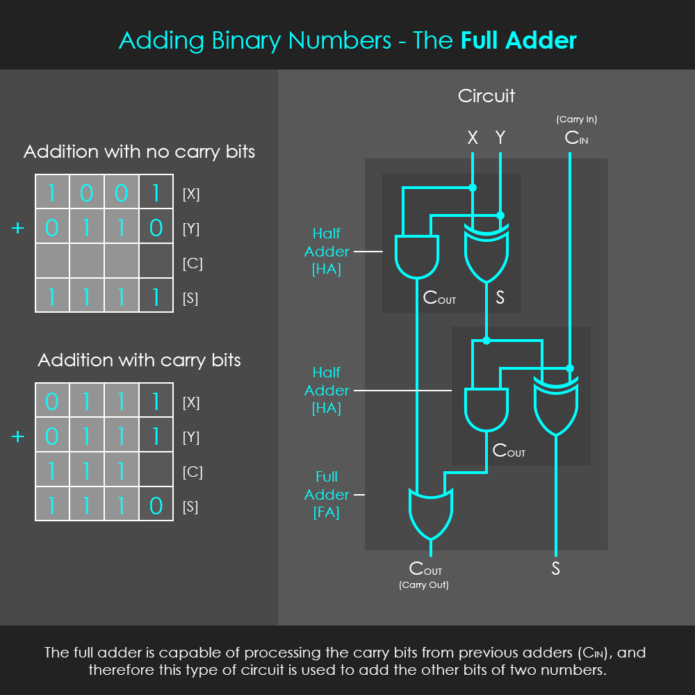
A full adder performs addition of two binary bits, and also processes the carry bit from the previous adder circuit. The carry out bit of a previous adder is used as the carry in bit for the full adder. The circuit of a full adder consists of two half adders, one performing the addition of X and Y, and the other half adder performing the addition of the first sum and the carry in bit. The outputs of both AND gates are fed into an OR gate that produces the carry out bit of the full adder. The sum of the second half adder is the sum of the full adder. The diagram shows the layout of a full adder circuit.
Adding 0+0, the sum of the first half adder is 0, and that is used as one of the inputs of the second half adder. With no carry in bit, the sum of the second half adder is also 0, serving as the sum of the full adder. No carry out bit is produced (0). Adding 0+1 or 1+0, the sum of the first half adder is 1, and therefore it depends on the carry in whether the second half adder produces a 1 sum with no carry out signal (when carry in = 0), or a 0 sum with a carry out signal (when carry in = 1). Adding 1+1, the sum of the first half adder is 0, and a carry out bit (1) is produced by the first half adder. If then carry in is 0, the sum of the full adder remains 0, whereas the sum of the full adder is 1 when the carry in signal is a 1.
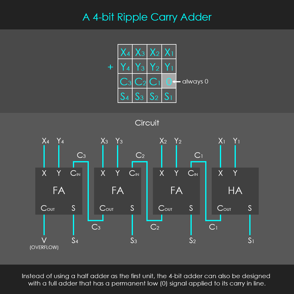
If binary numbers with several bits should be added, adder units can simply be chained together. For instance, a 4-bit adder can be designed by combining 4 adders. The adder for the least significant bits can be a half adder, and the other units are full adders. Each carry out signal is used as the carry in signal of the subsequent unit. In this design, the addition calculation starts with the least significant bits and completes as the carry signals ripple across the chain. For that reason, this design is also referred to as ripple carry adder. The last carry out that does not lead into another adder unit is called overflow and it indicates that the sum is too large to be represented in the output format. To prevent overflow from limiting the capacity of a calculator, the length of an output should be larger than the length of the operands. The following illustration shows the circuit of a 4-bit ripple carry adder. Although ripple carry adders can be used to build much larger chains (16 bit, etc.), they tend to become slower with increasing length. This is due to the fact that each adder stage can calculate its output only when the earlier stages have finished their calculations.
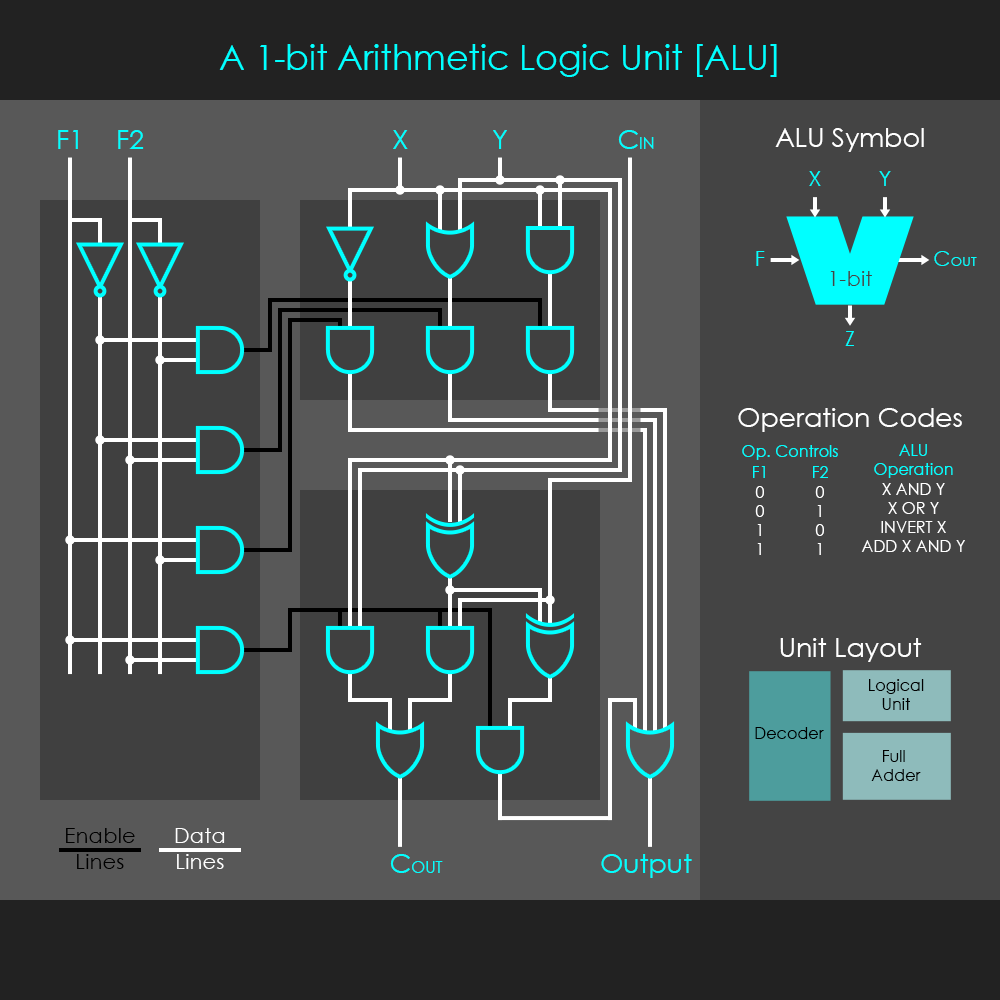
With only few components, a simple 1-bit ALU can be designed. The diagram shows an ALU that can perform one arithmetic operation (ADD X TO Y) as well as three logical operations (NOT X, X OR Y, X AND Y). The decoder on the left serves as a selector that only activates one of the enable lines at a time, so that only one operation result will be forwarded to the OR gate that leads to the output. The signal applied to the decoder is also called the operation code as it works as an instruction to the ALU on what to process.
A simple 4-bit ALU can be designed by linking four 1-bit ALUs together, called bit-slicing. The diagram shows that four 1-bit ALUs can be combined so that each carry out signal is used as the left slice’s carry in. The last carry out signal is an overflow flag indicating that the binary result is larger than four bits. All of these ALU slices share the same opcode signal line.
