A latch is a form of sequential circuit that has two stable logic states, high or low. A latch maintains its current state indefinitely until a different input signal is received at one of the inputs. Therefore a latch can be used as a memory device, and can store one bit of data.
There are two basic types of circuits used for latches. In an active-high circuit, both inputs are tied to ground (0) by default, and the latch is triggered by a high (1) signal on either of the inputs. Inversely, in an active-low circuit, both inputs are high (1) by default, and the latch is triggered by a low (0) signal on either input. For the purpose of the following explanations, it is assumed that all inputs to the latches are active high, unless otherwise indicated.
The illustration shows the circuit for an SR latch designed with NOR gates. Note that an SR latch can also be constructed with NAND gates, and those designs always have the S input on top and the R input below. An SR latch with NOR gates always has the R input on top and the S input below. In both designs, the output Q is always on top and the output Q-Inverted is always below. Q-Inverted is always the opposite of Q.
The SR latch consists of two NOR gates cross-coupled so that the output of each NOR gate is one of the inputs of the other NOR gate. As always with logic gate networks, power connections aren’t shown in the diagram. There are two inputs, an S input to set the latch, and an R input to reset the latch. On the output side, the latch is considered to be ‘set’ when Q is high (then Q-Inverted is automatically low), and ‘reset’ when Q is low (then Q-Inverted is automatically high). In order to trigger a latch to change its state, short pulses of signals are sufficient at the input lines.
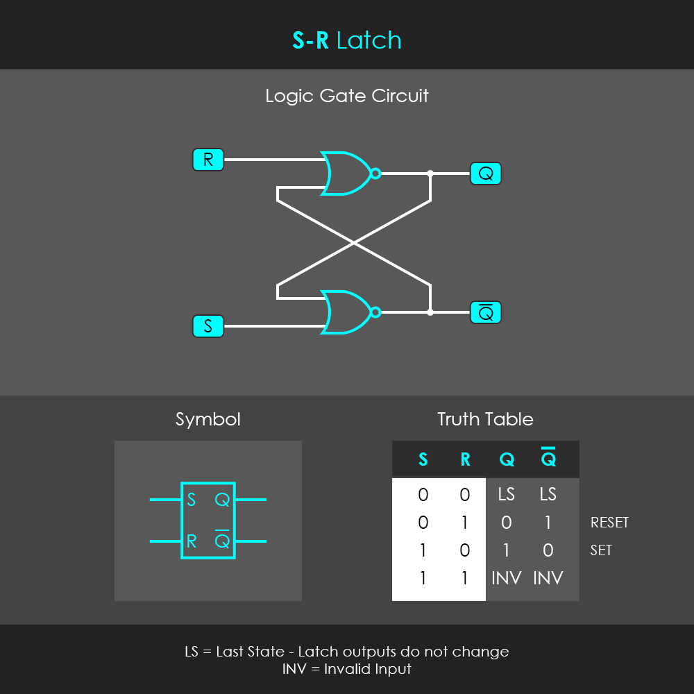
Initialization of the latch: When initializing the latch (starting up the circuit by applying power to all components), and having both inputs S and R low, the latch is in an unstable condition for a short moment because all of the gate inputs are low, turning both NOR gate outputs high at the same time. This is an unstable condition because both high outputs feed back into the inputs of both NOR gates, turning both outputs low again at the same time. These two low signals feed back into the inputs again and turn both outputs high again, causing an oscillation between the output states 1-1 and 0-0. Note that the definition of the outputs is Q and Q-Inverted which makes two identical values for Q and Q-Inverted an invalid state.
The latch is only stable when one gate output is high and the other gate output is low. Therefore, during initialization of a latch, the signals in both NOR gate circuits and their feedback loops are racing against each other. Tiny differences in signal speed (in the range of picoseconds) can occur from differences in wire lenths of circuits, from power fluctuations, or other imperfections. In this instance, it is assumed that the top NOR gate is slightly faster and turns the Q output high slightly earlier than the lower NOR gate. The high signal then runs through the feedback loop earlier and reaches the input of the lower NOR gate earlier, thus winning the race. The faster signal turns the output of the lower NOR gate low. This produces a stable condition because a low signal at the Q-Inverted output keeps both inputs at the top NOR gate unchanged, and interrupts the oscillation.
This timing-related phenomenon is called the ‘race condition’ and may sometimes take a few cycles of oscillation until the latch settles into a stable situation. Nonetheless, it is unpredictable whether a race condition causes the latch to stabilize in a set or reset state.
The latch is in the set state and stores a 1: It is supposed that Q is in the high (1) state. No signal is applied to the inputs. In this condition, the high output of the top NOR gate is also fed back to the lower NOR gate, which keeps the Q-Inverted output low (0). This is a stable condition of the latch, and the latch is storing a 1. While in the set condition, applying a high signal to the set input doesn’t change the state of the outputs, because the lower NOR gate already has one input high from the feedback loop, and a second high input leaves the gate output low.
Reset: While in the set condition, applying a high (1) signal to the reset input, the output Q of top NOR gate becomes low (0). This output is fed back to the input of the lower NOR gate, and the lower NOR gate turns the Q-Inverted output high (1). This high output of the lower NOR gate is fed back into the input of the top NOR gate. The high signal that was applied to reset the SR latch can then be removed so that the R input is low again. The output Q of the top NOR gate remains low. The latch has been reset and the output Q is low.
The latch is in the reset state and stores a 0: In this condition, the high output of the lower NOR gate is also fed back to the top NOR gate, which keeps the Q output low (0). This is a stable condition of the latch, and the latch is storing a 0.
Note that applying a high signal to the reset input doesn’t change the state of the outputs while in the reset condition.
Set: In order to store a 1 again, a signal must be applied to input S to set the latch. When applying a high (1) signal to the set input, the output of the lower NOR gate (Q-Inverted) turns low (0). This output is fed back to the input of the top NOR gate, and the top NOR gate output Q turns high (1). As the output Q is now high, this signal is fed back to the input of the lower NOR gate, which is already turned low due to the high signal at the set input. The signal that is applied to set the SR latch can then be removed so that the S input is low again. The output of the lower NOR gate remains low, and the output of the top NOR gate remains high. The latch has been set and is storing a 1 again.
Reset and Set at the same time: If two high signals are applied to both inputs S and R at the same time, the latch enters an invalid state. Both inputs high at the same time turns both outputs low, and feeds back two low signals to the inputs of both NOR gates. If the inputs turn low again at the same time, a race condition is induced, leading to an unpredictable result. For that reason, the truth table shows ‘invalid’ (INV) where both S and R are high at the same time.
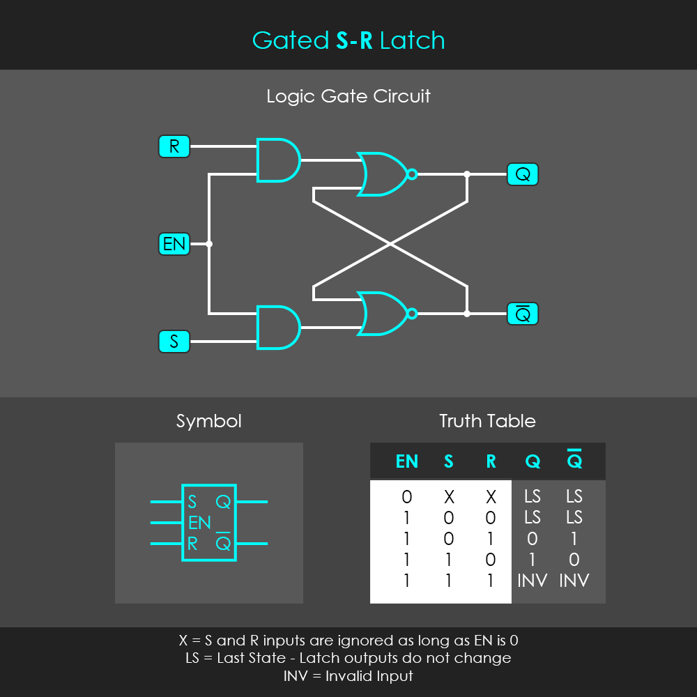
Since the SR latch is sensitive to its inputs all the time, it can be useful to enable or disable the inputs. An SR latch with enable (also known as a gated SR latch) allows the S and R inputs to be actively enabled or disabled by implementing an additional enable input. Therefore, two AND gates are connected to the original SR latch circuit as shown in the diagram.
When the enable signal is high (1), the circuit behaves like the normal SR latch as both AND gates directly pass through any S and R input signals. In this situation, the latch is said to be ‘open’ and the path from the inputs to the outputs is ‘transparent’. Hence the circuit is also referred to as a transparent latch. When the enable signal is low (0), the latch remains in its last state regardless of the S and R inputs. In this situation, the latch is disabled or ‘closed’ so that the outputs retain their last values independent of the inputs. In practice, the enable input may be named ENABLE, CLK, or CONTROL.
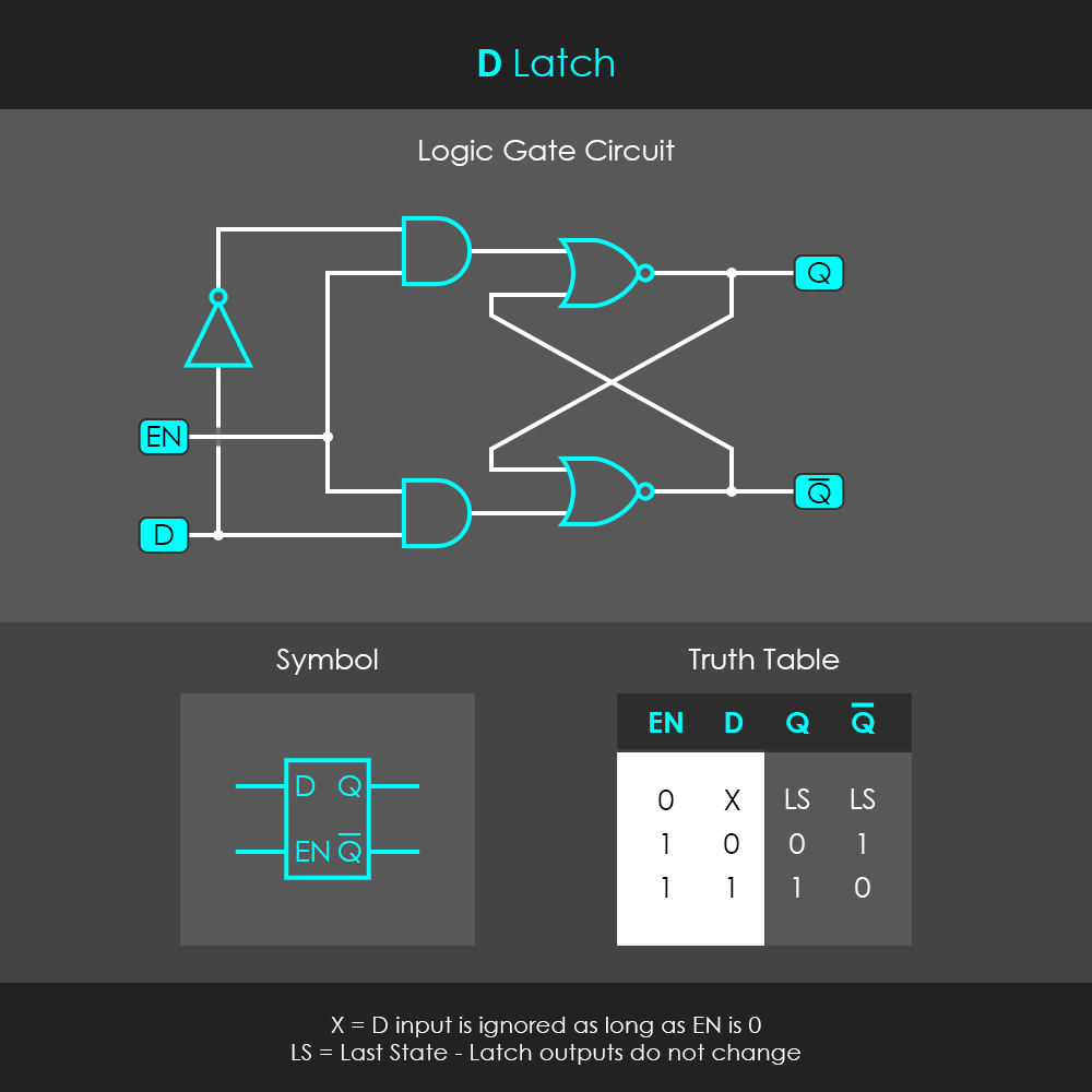
The disadvantage with the SR latch is that both inputs, S and R, must never be high at the same time, as this leads to an invalid state (Q and Q-Invert low at the same time), and ultimately to an unpredictable latch state when both signals are turned low again. This situation is prevented by using a D latch. An inverter is added between the original S and R inputs and a single input D (for data) is used as shown in the diagram. Notice that the placement of the inverter with respect to the Q output is such that the Q output follows the D input.
The inverter ensures that the input to the upper NOR gate is never identical with the input to the lower NOR gate. Whenever there is a high (1) signal on the D line, the latch turns into the ‘set’ condition (Q = 1). On the other hand, when there is a low (0) signal on the D line, the inverter turns the (original reset) input to the upper NOR gate high, and turns the latch into the ‘reset’ condition (Q = 0). This is a very useful circuit as it reads the information that is present in the D line and stores it in the Q output. For that reason, the D latch can be used as a memory unit that stores 1 bit of data. For the purpose of storing data, the output Q-Inverted can be ignored.
Again, the D latch shown in the figure has an enable input implemented. Only when the enable signal is high, output Q follows the input D. In this situation, the latch is open and the path from the input D to the output Q is transparent. Hence the circuit is also referred to as a transparent latch. When the enable input turns low, the latch is closed so that the output Q retains its last value independent of the D input.