A flip flop is a tiny device that can be used to store 1 bit of data. If the device needs a higher storage capacity in terms of the numbers of bits, the number of flip flops needs to be increased. The number of required flip flops is identical with the number of bits the device intends to store. Such a device that contains a certain number of flip flops is called a register.
The binary data stored in a register can be moved from one flip flop to another. Devices that allow such types of data transfers are called shift registers. A shift register is an array of flip flops in which the output of each flip flop is connected to the input of an adjacent flip flop. All flip flops share the same clock, so one clock cycle can shift all data by one position at the same time. Shift registers can have both parallel and serial inputs and outputs. The illustration shows these different types of inputs and outputs of shift registers. Each block represents one flip flop that can store 1 bit of data. Therefore, the array shown can store a total of 4 bits.

Depending on the circuit design, serial data can be shifted in two directions, left or right. This means that the left serial input can also be an output, and the right serial output can be an input. The various input and output options lead to the following categories of shift registers:
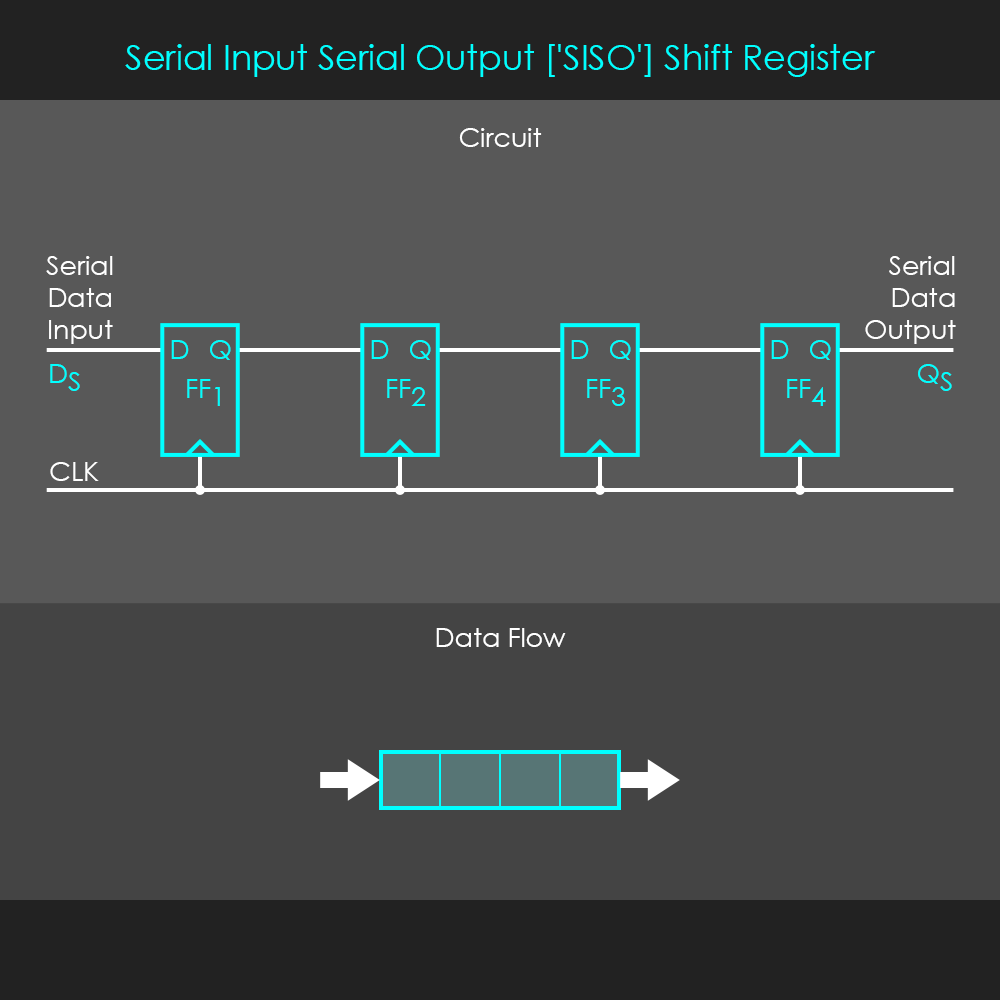
The circuit of a 4-bit serial input serial output shift register is simply a cascade of four flip flops connected in series as shown in the illustration. Data is fed into the shift register by the serial data input DS and gets shifted one position to the right by each clock cycle. The diagram shows a SISO shift register circuit that shifts data to the right.
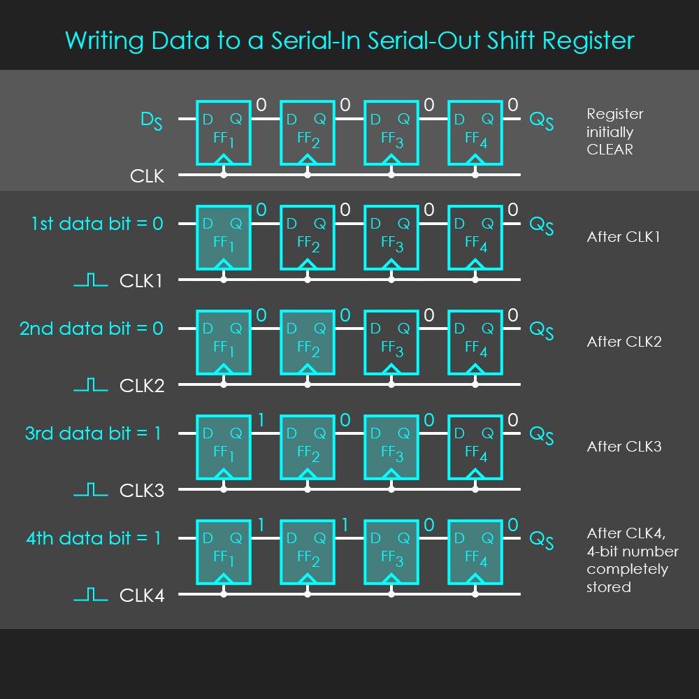
It is assumed that ‘1100’ is the sequence of 4 bits that needs to be stored in the shift register. It is also assumed that in the initial state the shift register is fully reset and stores ‘0000’ as its data content. When writing data to a serial input register, bits of data can only be written one after another, starting at the bit on the right (0). Four clock pulses load the register, and each bit moves one position to the right each time a clock cycle occurs.
The first bit of data (0) is applied to the DS line, and the first clock cycle (CLK1) writes that bit of data into the first flip flop. Then, the second bit of data (0) is applied to the DS line, and the second clock cycle (CLK2) shifts the data bit from the first flip flop into the second one, and simultaneously writes the new bit of data (0) from DS into the first flip flop. CLK3 and CLK4 shift their respective bits of data (1 and 1) in and store them in both flip flops on the left. After four clock cycles, the 4-bit number is completely stored in the shift register.
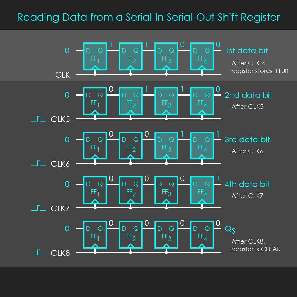
The readout process is similar as bits can only be read one after another. Four clock pulses unload the register, and each bit moves one position to the right each time a clock cycle occurs.
When the shift register is fully storing 4 bits, the output of the last flip flop shows the first data bit (0) at the output line QS so that subsequent units can already read it without a clock cycle required. Once the clock cycles (CLK5), all the data bits move one position to the right, so that the 1st data bit disappears, and the 2nd data bit (0) is shifted into the last flip flop and is shown at QS. On the next clock cycle (CLK6), the 2nd data bit disappears, and the 3rd data bit (1) is shifted into the last flip flop. CLK7 shifts the final 4th data bit (1) into the last flip flop. After CLK8, the shift register has completely unloaded the 4-bit number and is now empty. Any downstream register that is synchronized with CLK4-CLK7 can use the serial sequence of 4 bits for storing them. Note that unloading a register also allows it to write to it simultaneously, so the flip flops that become vacant during unloading can already store a new sequence of 4-bits.
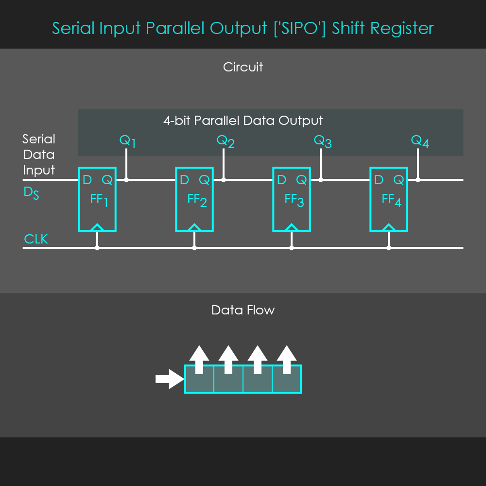
The serial input parallel output shift register has the ability to make all of its stored bits available at the same time. This is achieved by adding connecting wires to each of the flip flop’s outputs as shown in the diagram. When the shift register is completely loaded and stores a 4-bit sequence, no more clock cycles are required to unload the bits. The parallel outputs Q1-Q4 directly make the stored bits available for further processing by downstream parallel units.
A serial input parallel output shift register is often used as a serial-to-parallel-converter. Interestingly, the SIPO shift register is also a SISO shift register where Q4 can be used as a serial output.
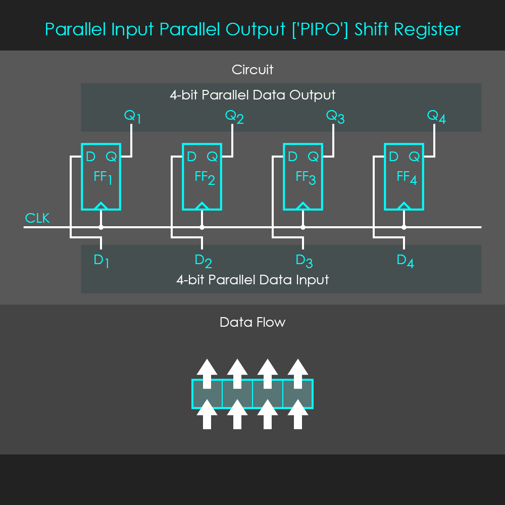
The parallel input parallel output is technically not a shift register as it cannot shift stored data bits between flip flops. It is nevertheless very useful to store a sequence of bits from a parallel data supply D1-D4, and make all of its stored bits available at the same time through its outputs Q1-Q4. One clock pulse is sufficient to store all of the input data bits in the flip flops and transfer these data bits to the outputs.
The parallel input serial output shift register allows to store a sequence of bits from the parallel data supply D1-D4, but then shift the stored bits to the right as in a SISO shift register. This can only be done by a multiplexer that selects whether a parallel data line or a previous output is connected with the following flip flop input D.

A signal is applied to the selector line so that the multiplexers connect the parallel inputs D2-D4 with the inputs D of the flip flops. Parallel input D1 doesn’t go through a multiplexer as no output of a preceding unit is connected to the first flip flop. In this condition, the first clock pulse stores the complete 4-bit sequence in the shift register.
To perform a serial readout, the signal on the selector line is reverted so that the multiplexers now connect all flip flop outputs Q to the inputs D. Then, the shift register behaves like a regular SISO shift register, and four clock pulses completely unload the shift register. A parallel input serial output shift register is often used as a parallel-to-serial-converter.
A universal shift register can store data from serial or parallel inputs, shift data in both directions, and output data through serial or parallel outputs. The circuit for a 4-bit universal shift register includes four D flip flops and four 4:1 multiplexers, and it is shown in the diagram.
A typical universal shift register has four modes of operation: Hold (which keeps the stored bits of data in the same position), shift left, shift right, and parallel load. Interestingly, the circuit doesn’t require individual modes to enable parallel or serial readout functions. This is because the stored bits of data are available at the parallel output lines at any time, and serial readout can be performed at Q1/QSL when shifting data to the left and at Q4/QSR when shifting data to the right.
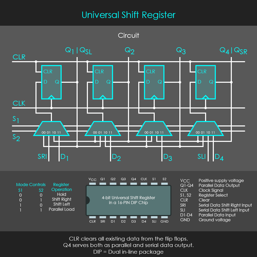
The multiplexers are the units that control which data line is connected to the inputs D of the flip flops. When the mode control signals S1 and S2 are 00, the circuit shows that all multiplexers connect the flip flops inputs D to their own outputs. This means that on each clock cycle, the flip flops are going to store the same bit that is already stored, and therefore the stored bit of data is held in position. When the control signals are 01, the multiplexers connect all the flip flops in a chain configuration that allows data to be shifted to the right. Looking at the flip flops (except the one on the far left), the multiplexer in their 01 settings connect the inputs D of the flip flops to the outputs Q from the adjacent flip flops to their left side. The flip flop on the far left has its input D connected to the SRI (serial right-shift input). When selecting 10, the multiplexers also connect all the flip flops in a chain configuration, but this time for data to be shifted to the left. Looking at the flip flops (except the one on the far right), the multiplexer in their 10 settings connect the inputs D of the flip flops to the outputs Q from the adjacent flip flops to their right side. The flip flop on the far right has its input D connected to the SLI (serial left-shift input). Finally, when the mode control signals S1 and S2 are 11, the circuit is set to use parallel inputs D1-D4 to store data in the flip flops. The multiplexers simply form connections between all inputs D of the flip flops with the parallel load connections D1-D4.
Universal shift registers are very useful circuits, and therefore they are also produced as individual microchips. The lower section of the diagram shows a 4-bit universal shift register in a dual in-line pin (DIP) chip package with 16 connector pins. In more complex integrated circuits, shift registers are deeply embedded in the overall system architecture so that none of the registers connectors are actually connected to the chip’s outside pins.