The microarchitecture level is a further abstraction where the overall interaction of all functional units is described. The abstraction lies in the simplification of schematics where only simple block diagrams and arrows are used, but auxiliary circuitry like multiplexers or tri-state buffers are usually not shown. Another simplification is that an n-bit bus line is often not drawn with n parallel lines, but is rather displayed as one line that is crossed by a small dash with the number of n bits written next to it.
In general, microarchitectures are typically categorized into two parts: The datapath which performs the calculations and microoperations (register transfer, arithmetic, logic, shifting) on data, and the control unit (or control path) which sends sequences of control signals to the datapath for processing. The figure below is a very general microarchitecture scheme that can represent fairly simple circuits (like a digital watch) but also very complex digital systems like modern multi-core CPUs.
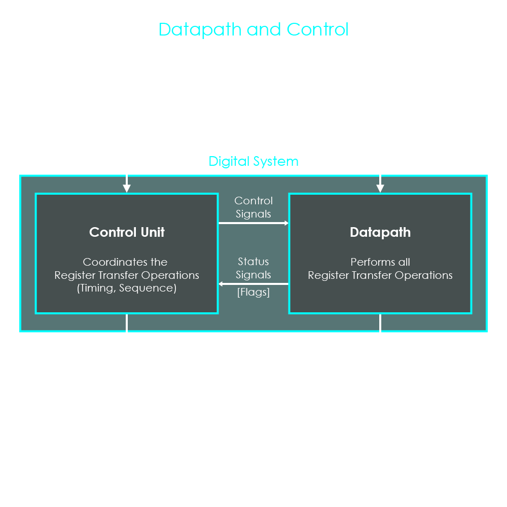
The control unit receives control inputs, also called instructions, and translates these instructions into control signals for the datapath. These control signals typically include register load signals, bus control signals (signals to bus drivers), and ALU opcodes. There is also a line for status signals, called flags, that includes feedback from ALU operations. Very common flags are the zero flag [Z] that indicates that a result of an arithmetic or logical operation was zero, and the carry flag [C] that indicates that the result of an operation was larger than a single n-bit word. The control unit also has control outputs to indicate whether an operation has been successfully processed. The datapath has data inputs where data to be processed is loaded into the datapath, and data outputs where all the processed results are issued to subsequent systems.
The next diagram is more detailed and it shows some of the structures within the control unit and datapath of a programmable central processing unit (CPU) as used in computers. Note that the datapath includes some of the auxiliary units like tri-state buffers for better descriptiveness. These will not be shown in later microarchitecture diagrams.
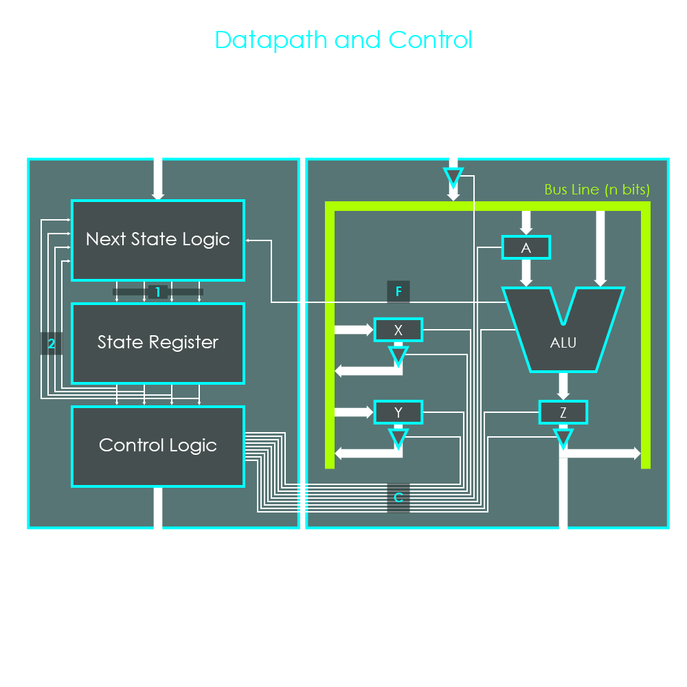
The datapath contains three types of units which can be categorized into storage units (registers), functional units (ALU, adders) that perform all the necessary operations on data, and interconnect units (buses) including their corresponding driver circuits (multiplexers, tri-state buffers). The datapath can also be described as the path that the input data follows in a CPU until it appears as an output.
Looking at the digital system above, here is how the datapath handles the flows of data when two binary numbers are added:
1. The first number is added to the bus: External circuitry addresses an external memory location where the first number is stored. This external memory information is applied to the data input line. The control unit activates the tri-state buffers (for an n-bit data line, n buffers are required) at the data input line so that external information is written to the bus. Note that the bus system cannot store information, so another register – for instance register X – is required to store the first number. Therefore, the control unit activates the load line for register X which loads the content of the bus and stores it in register X. After that, both the control line to activate the tri-state buffers at the data input line and the load signal for register X are disabled.
2. The second number is added to the bus: External circuitry addresses an external memory location where the second number is stored. This external memory information is applied to the data input line. The control unit activates the tri-state buffers at the data input line so that external information is written to the bus. This time, the content of the bus is stored in register A – also called the accumulator register – which has its outputs directly connected to one of the ALUs inputs. Note that there are no tri-state buffers required between the outputs of register A and the first ALU inputs due to the fact that its content is only used by the ALU, and therefore there is no conflict with other register outputs. The control unit activates the load line for register A which loads the content of the bus and stores it. After that, both the control line to activate the tri-state buffers at the data input line and the load signal for register A are disabled.
3. The two numbers are added: The ALU has two inputs. One input comes from register A, and the other input comes from the bus directly. Register A has its output permanently connected to the ALU, and therefore the ALU constantly received its first set of input signals. For the ALU to receive the second set of input signals, some information must be active on the bus. The control unit activates the tri-state buffers that connect the outputs of register X with the bus. This writes the content of register X onto the bus, and simultaneously applies the second set of input signals to the ALU. The control unit issues an operation code to the ALU which performs the desired operation.
4. The result is issued or stored: The control unit activates the load line for register Z which stores the sum of both numbers. After these steps, the result can either be written to the bus for further use in subsequent operations, or it can be issued to an external unit. Therefore, the control unit activates the tri-state buffers at the outputs of register Z, and its content can either be stored in another register that is connected to the bus, or can be read from external units.
The control unit includes circuits that issue instructions to the datapath to coordinate data transfers, operation selection, and other actions.
The control unit issues its instructions by activating only those functional units of the datapath that need to participate in a particular operation, and deactivating the ones that are not required at a given time. An instruction typically involves several steps within the datapath, so the control unit also performs sequencing and timing of single steps. In addition, the datapath also sends status signals back to the control unit so that a back and forth communication is established between these two sections of the digital system. The control unit is considered to be one of the most complex units of a CPU, and therefore the following descriptions on the control unit are kept to a minimum.
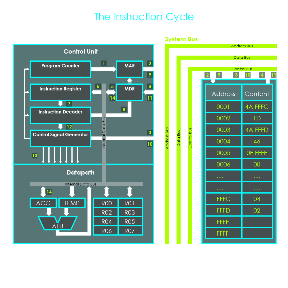
The instructions that need to be executed are stored within the system’s memory which is typically an external unit outside the CPU. In the memory, each piece of data has a unique storage location called the memory address. The CPU and the memory unit communicate via different bus lines, an address bus that carries information about storage locations, a data bus that carries the actual data values, and a control bus to enable or disable certain components. For instance, the CPU drives certain control bus signals that in turn enable or disable the memory unit, and determine whether a data value is read from a certain memory address or data is written into a certain memory address. Once data is read from the external memory, it is transferred into the CPU where the control unit translates these instructions into specific control signals. This is done by an arrangement of various components:
The program counter (PC) plays an important role in the sequencing of instructions. The program counter is a register that contains the memory address of the next instruction to be executed by the system. Once the next instruction address has been read by the other units of the system, the program counter’s content is being updated with a new instruction’s address. The new address is generated by an incrementer that always adds 1 to the current value of the program counter, and therefore increments the next instruction addresses by 1. When the system restarts or is reset, the program counter is usually reset to 0. A program counter is also referred to as an instruction counter, instruction pointer, instruction address register or sequence control register.
The instruction register (IR) holds the instruction that is currently being decoded by the control unit or executed by the datapath. For that reason, the IR is also called the current instruction register (CIR). Decoding and execution of an instruction can take several steps, and the IR holds the instruction during that time.
The instruction decoder is one of the most important parts of the control unit. It is a combinational circuit that has several inputs that correspond to the binary digits of an instruction. An instruction that needs to be processed is sent to the instruction decoder, and the instruction decoder then processes the state of all binary digits of the input signals to determine the required control lines.
The control signal generator is responsible for the timing and sequencing of control signals. For many instructions, the datapath must perform numerous individual steps. For instance, when two numbers need to be added, the addends (operands) have to be transferred into two registers next to the ALU (2 steps), the ALU has to be activated with the applicable opcode for addition (1 step), and the result has to be stored in another register (1 step). For this purpose, the control signal generator is the unit that generates the right sequence of control signals and sends these to the required functional units.
There are two more registers which are not part of the control unit in a stricter sense, but they constitute an important interface between the processor and the external memory:
The memory address register (MAR) is the register that holds the next memory address that the processor needs to access either for reading or writing. It is the control signals to memory that decide whether memory data from the selected address is written onto the data bus, or data from the data bus is written into memory at the selected address. The outputs of the MAR are connected to the system’s address bus which is outside the CPU, so that its content can be read by the external memory when activated.
The memory data register (MDR), also called memory buffer register or buffer register, holds the actual data that has been read from memory, or that needs to be written into memory. The MDR is therefore a two-way register. This means that it can either read information from the system’s data bus which is outside the CPU or write data onto that bus. Conversely, it can also read information from the internal data bus which is part of the integrated circuit, or write data onto that bus. The direction in which data flows is controlled by various bus drivers.
With these units (1-6), the control unit performs a series of data transfers known as the instruction cycle or also called fetch-decode-execute cycle.
The instruction cycle is the fundamental sequence of steps that a processor performs during operation. It is also known as the fetch-decode-execute-cycle and it is composed of three main phases:
In the fetch phase, the control unit requests an instruction from external memory, and transfers it into the CPU where it is stored in the instruction register (IR).
In this phase, the instruction that is stored within the instruction register is transferred to the instruction decoder. The decoder then interprets the binary instruction and arranges the next steps.
In the execute phase, the control signal generator issues a sequence of control signals to all circuits and units involved. Typical execution steps are transfers of data between CPU registers, ALU calculations, or data transfers between CPU and memory.
Every time an instruction cycle is complete, the CPU immediately starts a new cycle to process subsequent instructions stored in memory. For that reason, as long as any computer system is running, the CPU is constantly running instruction cycles, until the system is shut down.
A closer look reveals that the instruction cycle is a fairly detailed process, and some of its steps may vary depending on the type of instruction. In order to describe the instruction cycle more comprehensively, it is often divided into six phases. The illustration is a schematic that shows circuits and units involved in the instruction cycle, and the square brackets [] indicate the sequencing of control signals or data flows. The following descriptions explain the individual steps of an ‘LDA’ instruction cycle that loads a data value into the accumulator register.
The entire process starts with a register called the program counter (PC) which holds the memory address for the next instruction to be executed. [1]: The control unit transfers the program counter’s value (the next instruction’s address) to the memory address register (MAR) which is an interface to the external memory. [2]: The memory address register then places its value onto the system’s address bus that is also connected to the external memory unit. [3]: Then, the control unit sends a read signal along the system’s control bus which is also connected to the external memory unit. [4]: Upon receipt of the read signal, the memory unit uses the address signal present on the address bus, and places the binary instruction that is stored in the address onto the system’s data bus. This content is then read by the memory data register (MDR) which is also connected to the data bus, and which now holds a copy of the binary instruction that is stored in the external memory. [5]: In the next step, the instruction is transferred from the memory data register into the instruction register (IR). Once an instruction has been placed into the instruction register, the value in the program counter is incremented by 1 so that it points at the next instruction that needs to be requested from external memory once the instruction cycle starts all over again. The incrementation of the program counter’s value is carried out by an incrementer unit which is not shown in the diagram. This concludes the fetch instruction phase.
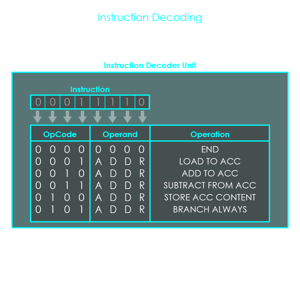
[7]: Once the instruction register contains a value, the instruction decoder is initiated and starts an interpretation of the instruction. An instruction is typically composed of two parts. The opcode (operation code) describes the operation that needs to be performed by the processor’s datapath, whereas the operand is the actual data that is used in the operation. The operand that is contained within the instruction can either be the actual data value (for instance a binary number that needs to be added to another number), or the address where the actual data value can be found in the external memory unit. The diagram shows the format of a simple 8-bit instruction.

During the instruction decode phase, the decoder unit translates the opcode into unique decoder output signals that will be further processed by the control signal generator. The diagram is an example of different opcodes and their meanings.
In this phase of the instruction cycle, also called address generation, the instruction decoder evaluates the memory address of the operand that is required for the operation. If an instruction does not require additional memory access (for instance an instruction for an internal data transfer between two CPU registers where no operands need to be loaded from memory), the instruction can be directly interpreted and forwarded to the signal generation unit for execution [12]. In the case of an instruction that does require additional memory access (for instance an instruction to load an operand from memory into an internal CPU register), the fetch operand cycle must be carried out.
[8]: In case this phase is required, the control unit loads the memory address register (MAR) with the address that was determined during the evaluate operand address phase. Then, another fetch cycle [9], [10], [11] reads the required operand from external memory, and places it into the memory data register (MDR), from where it can be used for the execute phase. [12]: In this case, too, the instruction decoder forwards an internal signal to the control signal generator.
When reaching this phase, every prior step of the instruction cycle has prepared the execution of the instruction: The instruction decoder has interpreted the opcode so that the control signal generator is set accordingly, and the operand is available in the memory data register. [13], [14]: The control signal generator issues a sequence of control signals to transfer the content of the memory data register into the accumulator. Note that the LDA instruction does not involve any ALU operation, but it is a very common instruction to prepare further execution phases like addition of two values. After the value was transferred to the accumulator, the execution phase ends.
This last phase transfers any result of an ALU operation into the accumulator register from where it can be used for further operations, or into an address of the external memory. If there is no result that has been computed by the ALU, this stage is not carried out. Once the last stage of the instruction cycle is complete, the control unit immediately starts a new cycle by reading the value of the program counter which already points to the memory address of the next instruction.
Although this was not actually mentioned in the description, all steps within the instruction cycle are carefully synchronized with the clock of the integrated circuit. In simpler CPUs, the instruction cycle is executed sequentially so that each instruction is completed before the next one is started. In today’s highly optimized CPUs, the instruction cycles are executed concurrently, and often in parallel, through an instruction pipeline. An instruction pipeline allows a CPU to start fetching, decoding and executing the next instruction before the previous one has finished.
The following section describes how a simple program with six instruction cycles implements the addition of two numbers that are stored in the external memory. The list below contains these six instructions written in assembly language that represent the short program for the addition. Please note that the instruction codes (4A, etc.) are completely arbitrary and and may deviate in reality.
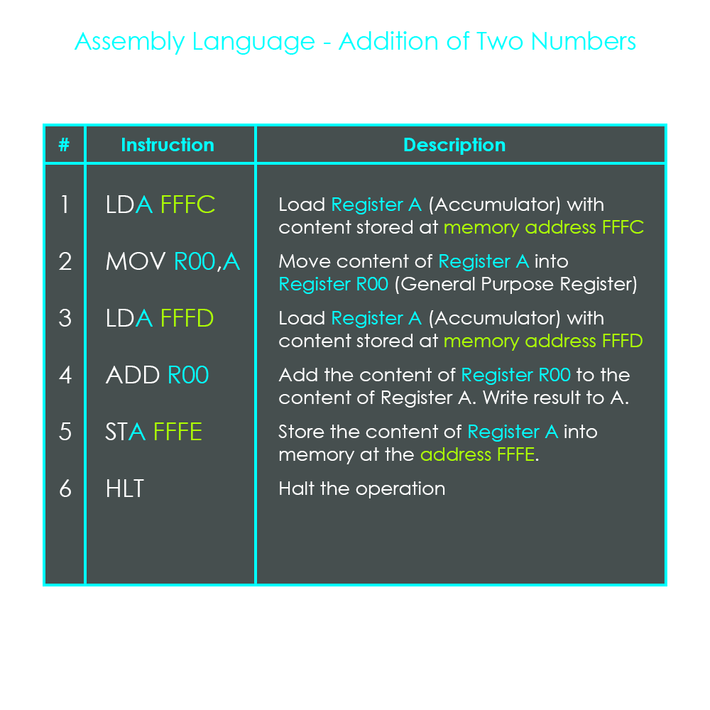
0001 is the address where the first instruction (4A FFFC) is stored in memory. 4A is the hexadecimal representation of the binary number 01001010, the opcode for the operation to load an operand from memory (depending on type of CPU). FFFC is the hexadecimal representation of the binary number 1111111111111100, the address where the first operand is stored in memory. The first instruction’s address 0001 is stored in the program counter and is copied into the memory address register. The address is then placed onto the address bus where it can be received from the external memory. The control unit then sends a read signal to the system’s control bus and the signal is received by the external memory. The external memory is now set to read information, and the instruction LDA FFFC that is stored in the memory address is now placed onto the system’s data bus from where it is transferred to the memory data register. After this step, the access to external memory can be deactivated again by the control unit, and the content is still available in the memory data register. The data received by the memory data register now gets copied into the instruction register. The instruction has now been fetched from memory and the program counter gets incremented by 1. The instruction that is stored in the instruction register is decoded. The opcode is interpreted to load an operand from memory, and the control unit prepares this step accordingly. The first operand’s address FFFC is placed into the memory address register, and another fetch cycle loads the value that is stored at memory location FFFC into the memory data register. When the value stored at FFFC has been copied into the memory data register, it is placed onto the internal data bus of the integrated circuit, from where it is written into the accumulator register. This ends the first instruction cycle.
The program counter now points at memory address 0002 where the second instruction (1D) is stored in memory. 1D is the hexadecimal representation of the binary number 011101, the opcode for the operation to move the accumulator’s content into the register R00. The system fetches the instruction (details can be found in the first instruction cycle) and transfers it in the instruction register. The program counter gets incremented by 1. The instruction that is stored in the instruction register is decoded. The opcode is interpreted to move the content that is stored in the accumulator to register R00 which is one of the general purpose registers of the CPU. The accumulator places its content onto the internal data bus from where it is transferred to register R00. This ends the second instruction cycle.
The program counter now points at memory address 0003 where the third instruction (4A FFFD) is stored in memory. 4A again is the opcode to load an operand from memory (depending on type of CPU). FFFD is the hexadecimal representation of the binary number 1111111111111101, the address where the second operand is stored in memory. The system fetches the instruction (details can be found in the first instruction cycle) and transfers it in the instruction register. The program counter gets incremented by 1. The instruction that is stored in the instruction register is decoded. The opcode is interpreted to load an operand from memory, and the control unit prepares this step accordingly. The second operand’s address FFFD is placed into the memory address register, and another fetch cycle loads the value that is stored at memory location FFFD into the memory data register. When the value stored at FFFD has been copied into the memory data register, it is placed onto the internal data bus of the integrated circuit, from where it is written into the accumulator register. This ends the third instruction cycle.
The program counter now points at memory address 0004 where the fourth instruction (46) is stored in memory. 46 is the hexadecimal representation of the binary number 01000110, the opcode for the operation to add the content of register R00 to the content of register A (accumulator) via the ALU. The system fetches the instruction (details can be found in the first instruction cycle) and transfers it in the instruction register. The program counter gets incremented by 1. The instruction that is stored in the instruction register is decoded. The opcode is interpreted to add the content of R00 to the content of register A. The value of register A is already in the correct position as the register’s output is directly connected to an input of the ALU. The value of register R00 is placed onto the internal data bus of the integrated circuit, from where it is written into the temporary register (TEMP). Once both registers A and TEMP are filled, the ALU performs the addition, and issues the result at its output. The ALU’s output value is stored in the accumulator. This ends the fourth instruction cycle.
The program counter now points at memory address 0005 where the fifth instruction (0E FFFE) is stored in memory. 0E is the opcode to store a value in memory (depending on type of CPU). FFFE is the hexadecimal representation of the binary number 1111111111111110, the address in memory where the data value should be stored (destination address). The system fetches the instruction (details can be found in the first instruction cycle) and transfers it in the instruction register. The program counter gets incremented by 1. The instruction that is stored in the instruction register is decoded. The opcode is interpreted to store the content of register A (06) to the external memory at address FFFE. The destination address is transferred to the memory address register from where it is placed onto the system’s address bus. The content of register A is placed onto the internal data bus of the integrated circuit, from where it is written into the memory data register. The memory data register places its content onto the system’s data bus. The control unit then sends a write signal to the system’s control bus and the signal is received by the external memory. The external memory is now set to store information, and the data (06) that is stored in the memory data register is now placed onto the system’s data bus. The external memory now stores the result of the addition (06) at the address FFFE. This ends the fifth instruction cycle.
The program counter now points at memory address 0006 where the sixth instruction (00) is stored in memory. 00 is the opcode to halt the processing (depending on type of CPU). The system fetches the instruction (details can be found in the first instruction cycle) and transfers it in the instruction register. Once this instruction has been fetched and decoded, the CPU stops incrementing the program counter, and halts the operation. This command is typically used at the very end of a program. This completes the addition of two numbers.
The 8085 is an 8-bit microprocessor designed by Intel and introduced in 1976. The chip was used in various computer systems of the 1970s, in office typewriters, oscilloscopes, and other systems. A specially flight-qualified (radiation hardened) version of the Intel 8085 was used for several NASA space missions in the 1990s and early 2000s, including for the NASA Mars Pathfinder lander that was launched from earth in 1996. The image is a microarchitecture diagram of the components and circuits inside this very popular CPU.
The diagram doesn’t show the realistic arrangement of functional units on the chip die but only the systematic connections between the individual units. It is easy to see which of the units are part of the datapath category and which ones are part of the control unit. The Intel 8085 has a set of six general purpose registers (B, C, D, E, H, and L). Each of these can store eight bits of information. Interestingly, these can also be combined as register pairs (BC, DE, and HL) to store 16 bits of information and to participate in 16-bit operations. These general purpose registers are accessible by a user, so they can be addressed by instructions such as MOV D,A. Registers W and Z are two 8-bit temporary registers that are again either two separate 8-bit registers or a combined 16-bit register. A special characteristic of these temporary registers is that they are not accessible to the user because they are exclusively used for the internal operation of the CPU. Note that the unit called ‘Address Buffer’ is the memory address register (MAR), and the unit called ‘Data/Address Buffer’ is the memory data register (MDR).
