The circuit level is a level of abstraction that makes it irrelevant to think about the physical structure of individual transistors with all their different materials and specialties. Instead, transistors are only thought of as small switches and a circuit designer only needs to know their general working principles. For instance, on the circuit level, a designer only needs to know that an N-MOS transistor turns on (and closes the circuit) when the voltage at the gate terminal is high. The designer of a circuit doesn’t need to think through the properties of n-type and p-type silicon and the formation of an n-channel. For that reason, the transistor symbols have been created to allow circuits to be designed more clearly.
An electrical circuit is a network of electrical components such as power sources, resistors, switches, transistors, light emitting diodes, and others. When the circuit is closed, this network always consists of a closed loop, allowing charge carriers to flow through the components (called the ‘load’ of the circuit) and return to their power source.
In integrated circuits, the power supply is always provided from external sources, for instance a computer’s power supply unit. The main power supply unit provides power to all components of the appliance through a network of power lines, conductive tracks called ‘power rails’, that are on or inside the appliance’s printed circuit board.
For its own voltage supply, every microchip has at least two power supply pins that direct the external supply voltage into the chip. One is always the positive supply voltage pin, labeled VCC or VDD. This one is connected to the positive power supply rail of the appliance’s printed circuit board. Inside the chip, the positive power supply is distributed to the required areas through internal power rails. There are industry standard voltage levels for integrated circuits with supply voltages from 0.6V up to 12V.
Another pin is always the ground pin, labeled GND. This one is connected to the ground rail of the appliance’s printed circuit board. The ground rail usually is the most negative voltage level (typically 0V), and is the return path of an electrical circuit. The ground rail inside the microchip leads away from all the tiny circuits to the ground pin of the microchip, into the ground rail of the appliance’s printed circuit board, effectively closing the circuit. Circuit designers often use VEE or VSS instead of GND to indicate that the respective rail has the most negative voltage of the entire integrated circuit. There can be some exceptions, but in most cases, the lowest voltage in an integrated circuit is 0V, and therefore equivalent to GND. For that reason, the following explanations and illustrations use GND as the identifier for the most negative supply voltage in a circuit.
The following explanation gives an overview of the power supply names depending on the type of components in a circuit.
The labels VDD and VSS are mainly used in applications where field effect transistors (N-MOS and P-MOS, in combination called CMOS) are combined to a circuit. The letters D and S refer to drain and source. It must be noted, however, that VDD is not only connected to drain terminals, and VSS is not only connected to source terminals of field effect transistors. In integrated circuits using CMOS technology, drains and sources can be connected to both types of power rails. This depending on the type of transistor. N-MOS transistors typically have their D terminal connected to the positive rail VDD, while P-MOS transistors have their S terminal connected to VDD.
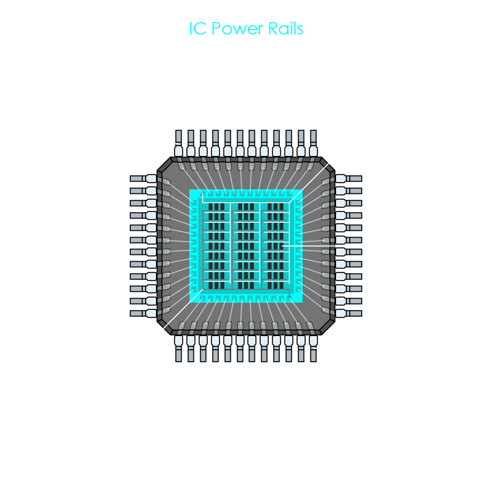
The labels VCC and VEE are mainly used in applications where BJT transistors (NPN and PNP) are combined to a circuit. The letters C and E refer to collector and emitter. Again, in real-life circuits, collectors and emitters can be connected to both power rails. Unfortunately, the labeling of the pins may also vary by the manufacturer, and so there are some CMOS microchips that also have VCC as their positive power pin. Integrated circuits usually use direct current sources instead of alternating current. This means that the polarity of power supply rails and ground rails will always remain the same while in operation. Today’s microchips consist of billions of transistors, and all of them have to be supplied with power. To achieve full coverage of the chip area with power, a complex distribution network is integrated in each microchip so that each transistor is connected to positive supply voltage and ground. The distribution network forms millions of individual circuits. The following image is a schematic representation of such a power distribution network.
In order to make sense of the following chapters, it is helpful to look at individual circuits using Bipolar Junction Transistors and Field Effect Transistors.

The illustration (left) shows two different states of a circuit that is using an NPN Bipolar Junction Transistor. Power is supplied from the VCC and GND rails where the NPN transistor is connected to. Note that the collector (C) of the NPN transistor is connected to the VCC rail. To indicate whether the transistor is in the off or on state, an LED (light emitting diode) is arranged between the emitter and ground. If the transistor is in the on state, the main current will flow from the VCC rail into the collector and out of the emitter of the transistor, through the LED and back into the ground rail. To protect the LED from receiving too much current, there is a current limiting resistor (R1) added within the main current. There is another resistor (R2) to limit the current that flows through the base and emitter terminals of the NPN as there is only a very small current required to activate the transistor. In option 1, the switch is open, and therefore no current flows through base and emitter, which keeps the transistor in its off state. Therefore, no main current is being established, and the LED remains off. In option 2, the switch is closed, and this time a small base current flows through the transistor, turning it into the on state. Now, the main current is switched on by the transistor, and the LED lights up.

The illustration (left) shows two different states of a comparable circuit. The only difference is that this circuit uses an N-MOS Field Effect Transistor instead of an NPN Bipolar Junction Transistor. Power is supplied from the VDD and GND rails. The drain (D) of the N-MOS transistor is connected to the VDD rail. Again, an LED is used to indicate whether the main current is on or off. The current limiting resistor (R) to protect the LED from overheating is located at the same position. However, with a Field Effect Transistor, there is no R2 required. The reason this circuit works without R2 is because an FET is a voltage controlled device, and no current will be established between the gate and the source terminals. The presence of a positive voltage itself at the gate terminal is sufficient to turn the FET on. In circuits using only FETs and no LEDs, no resistors are required at all, which is an advantage in design. In option 1, the switch is open, and therefore no positive voltage is applied to the gate, which keeps the N-MOS device in its off state. No main current flows, and the LED remains off. In option 2, the switch is closed, and the VDD voltage is applied to the gate, turning the N-MOS device on. Now, the main current is switched on, and the LED lights up.