On the device level, the smallest units within an integrated circuit can be found: Transistors. While the introduction has already mentioned transistors as being a fundamental component of microchips, understanding their structure and operating modes is the basis for other levels of abstraction.
A transistor is a device that uses smaller input signals to regulate larger current flows. Transistors have these general modes of operation:
It depends on the transistor type what is required to switch it on or off, but it is typically a minimum current established between two pins of the transistor or a voltage applied between two pins. Some of the illustrations further below explain this in more detail.
The ability to amplify analog signals is a required effect in many audio and radio applications. In digital circuits, however, signals consist of ‘1’ and ‘0’ which are realized by the presence of either full supply voltage (for instance 12V = ‘1’) or ground voltage (0V = ‘0’). Therefore, transistors as used in digital integrated circuits do only act in the cut-off region (completely off) or saturation region (completely on). For that reason, transistors in digital integrated circuits can be imagined as simple switches that either open a circuit (switch is off) or close it (switch is on).
There is one technicality that is important to know: In electronics, there are two concepts of current. Conventional current flows from the positive terminal, through the circuit to the negative terminal of the source. This is because for the conventional current it is assumed that the charge carriers are positive. Electron flow is what actually happens and electrons (always negatively charged) flow from the negative terminal, through the circuit and into the positive terminal of the source. This may appear very confusing, but in reality, it makes no difference which way current is flowing as long as it is used consistently. A flow of positive charges gives the same electric current, and has the same effect in a circuit, as an equal flow of negative charges in the opposite direction. Especially when thinking about switches that either open or close a circuit, the direction of current flow does not affect how the switches work. Throughout this article, conventional current is used unless otherwise indicated.
Over the last decades, numerous different types of transistors have been developed and optimized. In the early stages of transistors, germanium was a popular semiconductor material that was used in transistor production. During the 1960s and 1970s, germanium was gradually replaced by silicon due to several reasons. There are some advantages of silicon that made production and handling of transistors easier. In rare cases for special applications, gallium arsenide is used as a compound semiconductor material as it has some better properties for high frequency applications.
Today, transistors are categorized depending on their structure. As each type of transistor has its own characteristics, there are some devices with very specialized purposes. Some transistors are designed primarily for amplification purposes, some are designed for switching purposes and some transistors are designed for both amplification and switching purposes. Depending on their structure, transistors can be categorized into one of the two main types Bipolar Junction Transistor (BJT) and Field Effect Transistor (FET). The diagram summarizes the main transistor classifications. This article will only focus on Bipolar Junction Transistors (BJT) and Enhancement Mode Metal Oxide Field Effect Transistors (MOSFET).
The starting material for almost all transistors is silicon, a semiconductor material which has very special electric characteristics. In its pure form, silicon does not conduct electricity very well. However, by a rather complicated process called doping, impurities are injected into the material, effectively adding or removing electrons from the silicon. If electrons (which are always negative) are added, this type of silicon is referred to as n-type (negative type) silicon. If electrons are removed, this type of silicon is called p-type (positive-type) silicon.
If a layer of n-type silicon is next to a layer of p-type silicon, these two different zones form a connection that is called the p-n-junction. The special property of the p-n-junction is that it is conductive in one direction (if a minimum voltage is applied in one way) but blocks the flow of electricity in the opposite direction (if a minimum voltage is applied in another way). Conductivity of a p-n-junction can also be increased if an electric field is applied. To keep the focus of this article on integrated circuitry, silicon doping and the functional principles of p-n-junctions have been intentionally left out.
Bipolar junction transistors are current-controlled devices. If a small amount of current flows through the base, a BJT transistor allows a larger current flow between the emitter and the collector. It depends on the type of BJT in which direction current needs to flow through the base in order to turn the transistor on. The following chapters are taking a closer look into the construction and operation of NPN and PNP bipolar junction transistors.
All bipolar junction transistors are fomed by three alternating layers of silicon, either a layer of p-type silicon inbetween two layers of n-type silicon (NPN type) or a layer of n-type silicon inbetween two layers of p-type silicon (PNP type). They use both positive and negative charge carriers, hence the name bipolar. All bipolar junction transistors have three terminals, called emitter, base, and collector. The following diagram shows the schematic structures and electrical symbols for both NPN and PNP transistors.
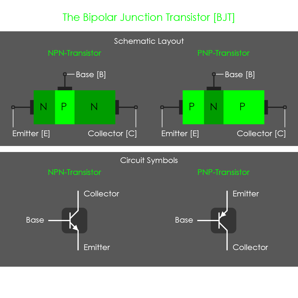
The NPN transistor is one of the two designs of bipolar junction transistors. The name NPN describes the sequence in which the differently doped silicon layers are arranged. An NPN transistor is turned on when a minimum (conventional) current is flowing into the base and out of the emitter. This is usually the case when the emitter is grounded (0V) and a positive voltage higher than 0.6V is applied to the base. When there is another positive voltage (typically the full source voltage) applied to the collector, a current flowing between the base and the emitter turns the NPN transistor on and allows current to flow from the collector to the emitter. Looking at electron flows, the only source of electrons is the grounded emitter. Only when a positive voltage is applied to the base, electrons are allowed to flow into the emitter and out of the base, which opens the transistor for more electrons to flow into the emitter and out of the collector.
The PNP transistor is another design of bipolar junction transistors. A PNP transistor is turned on when a minimum (conventional) current is flowing out of the base. Therefore, the base voltage must be at least 0.6V lower than the emitter voltage, so typically the full source voltage is applied to the emitter and the base is grounded in order to open the transistor.
Due to consistency reasons, circuits are usually drawn with the source power line on top, and the ground line below. For that reason, the symbol for a PNP transistor is typically flipped upside down to have the emitter (positive voltage) on top.
For integrated circuits, transistors are being produced in a planar design so that they have all their electrically active areas (connector terminals) on the surface of the silicon substrate. The diagram shows realistic cross-sections of both NPN and PNP transistors in a planar design.
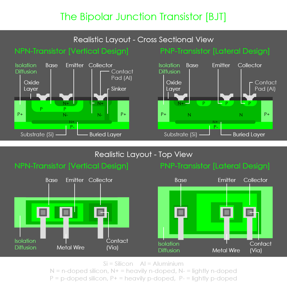
The layout of the planar NPN transistor (left part of diagram) is called vertical. This is due to the fact that the emitter, base and collector layers are arranged vertically on top of each other. The current flow in the device is also vertical, emitter through base and collected at the bottom by the buried layer that is directly connected with the collector by a sinker structure. NPN transistors with vertical design are considered to have good electrical properties.
Unfortunately, good PNP transistors are not available in a vertical layout. The only PNP devices available are either substrate PNPs and lateral PNPs. The substrate PNP uses the P-type substrate as the collector. The base region is mostly the N-well region and the emitter region is the P-type diffusion at the surface. The lateral PNP (right part of diagram) is formed by two closely located P-type diffusions, usually two concentric geometric shapes (circles, squares, etc.). The inner P-type diffusion is the emitter and the outer P-type diffusion is the collector. The N-Well in between forms the base. The current flow in this transistor is horizontally at the surface.
None of the PNP transistors can match the performance of the vertical NPN transistor. In addition, NPN transistors are cheaper in production and smaller in scale. Another reason is that it is more convenient for circuit designers to have the emitter tied to ground so that the control signal is always relative to ground. At a PNP transistor, the control signal has to be lower than the emitter for the transistor to turn on. In this setup, the emitter becomes the common reference for the control signal, and the collector is always connected to the most negative power supply rail. For these reasons, NPN type transistors are more popular than PNP types.
Field Effect transistors are voltage-controlled devices. They only require voltage applied to the controlling terminal to turn the FET either on or off. The voltage applied induces an electric field (instead of a current) to control the flow of current through the device.
The terminals of field effect transistors are called source, drain and gate. These roughly correspond to the emitter, collector, and base terminals of bipolar junction transistors. The names of the terminals originate from their functions. The gate terminal may be thought of as controlling the opening and closing of a physical gate. Field effect transistors are also known as unipolar transistors since they involve single-carrier-type operation. That is, FETs use positive or negative charge carriers in their operation, but not both.
Today’s integrated circuits mostly use MOSFETs, a special type of FET, for their operation. MOSFET stands for metal oxide semiconductor field effect transistor and the name refers to its fabrication process where a controlled oxidation is applied to the semiconductor material, typically silicon. Depending on their arrangement of n-doped and p-doped silicon areas, there are N-Channel-MOSFETs and P-Channel-MOSFETs.
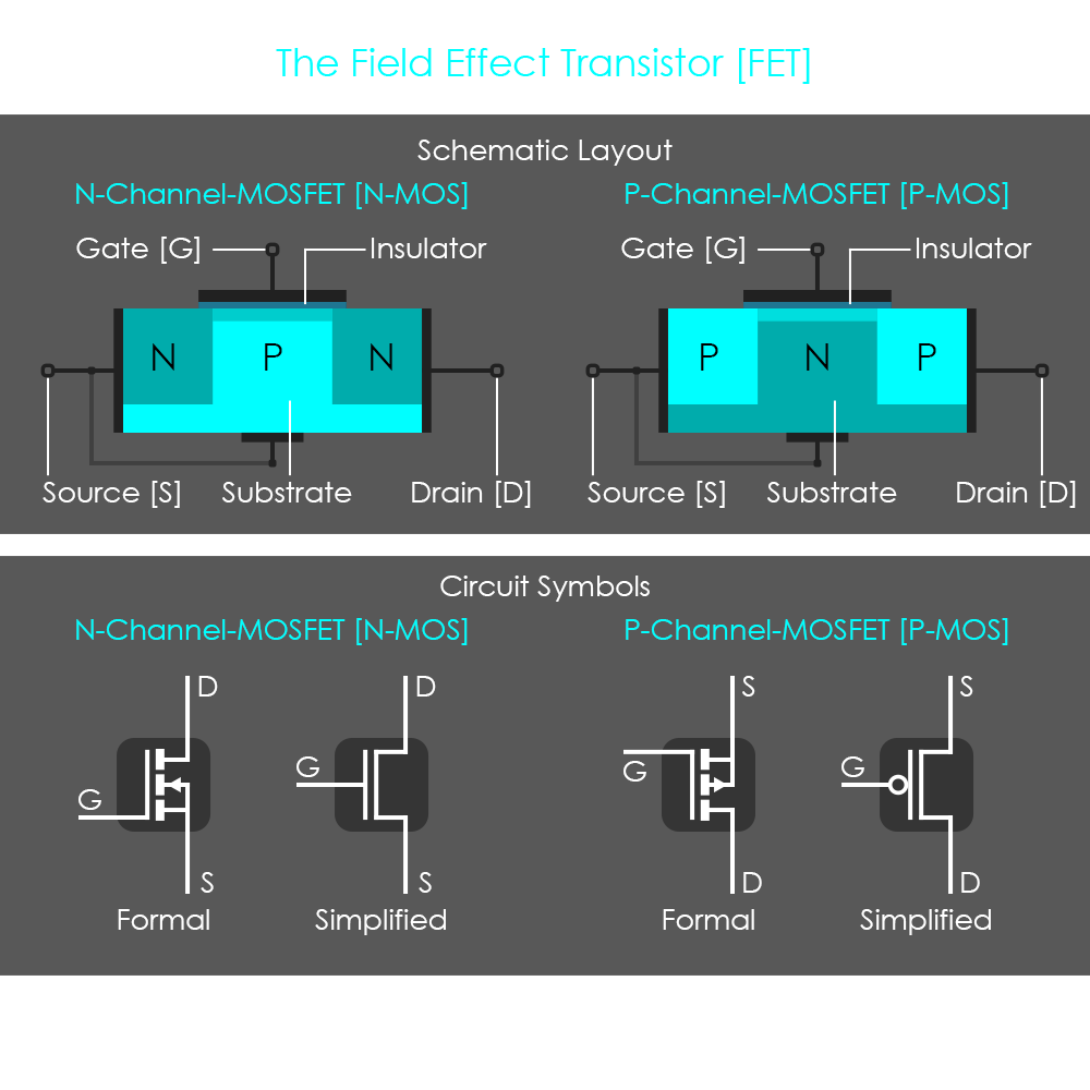
The N-Channel-MOSFET uses p-doped silicon substrate and has two n-doped silicon regions implanted with some space inbetween. One of the n-type regions is connected to the source terminal, the other n-type region is connected to the drain terminal. The entire setup is very similar to an NPN transistor, but the specialty with FETs is that the gate terminal is not directly connected with the silicon substrate. Instead, there is an insulation layer (silicon oxide) separating the substrate from the gate contact and prevents any current from flowing between the substrate and the gate. The gate consists of some bulkier metal plating so that many charge carriers can aggregate in there. A positive voltage applied to the gate causes the metal plating to become positively charged. This in turn induces an electric field and attracts electrons from the p-substrate to move into the direction of the gate. As they are ultimately blocked by the insulation layer, they accumulate directly below the silicon oxide insulator and form a negatively charged channel (n-channel, seen as a slightly darker blue region within the P-type substrate), also referred to as inversion layer. This n-channel effectively connects both n-type regions and allows a current to flow from the source to the drain.
As seen in the schematic, there is a fourth contact terminal, connected to the substrate. This terminal is called body, base, bulk, or substrate. This fourth terminal serves to calibrate the transistor while in operation:
The gate voltage creates the n-channel and also controls the channel width. However, the gate can only work effectively if the P-substrate is at a low voltage. Technically spoken, the gate potential is measured relative to the substrate potential, and the channel is formed in the substrate material. Therefore the MOSFET behavior depends strongly on the substrate (body) potential. This means that the substrate connector does not add any functionality, but actually ensures reliable operation. In most real-life applications, the substrate gets internally connected to the source during production, and therefore this fourth terminal will not be shown in later schematics.
The operation of an N-MOS transistor can be summarized as follows:
The P-Channel-MOSFET uses n-doped silicon substrate and has two p-doped silicon regions implanted with some space inbetween. The p-type regions form the source and drain of the P-MOS. Again, there is an insulation layer (silicon oxide) separating the substrate from the gate contact and prevents any current from flowing between the substrate and the gate. A P-MOS transistor is being activated when a negative voltage is applied to the gate. This causes electrons to aggregate inside the metal plating. This also induces an electric field, but this time repels electrons from the p-substrate and pushes them away from the insulation layer. This forms a positively charged channel (p-channel, seen as a slightly lighter blue region within the P-type substrate) where positive charge carriers can move freely between the source and the drain.
In P-MOS transistors, the body terminal is also internally connected to the source which is typically the higher voltage applied to the transistor. As the gate potential is measured relative to the substrate potential, the channel is only formed when there is a negative charge in relation to the substrate. Again, this fourth terminal is not shown in later schematics.
The operation of a P-MOS transistor can be summarized as follows:
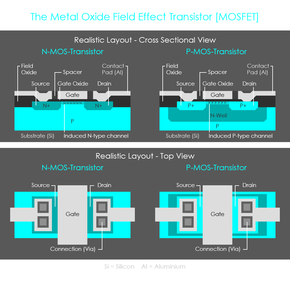
Again, for MOSFETs to be used in integrated circuits, they must have all their connector terminals on one side of the surface, and therefore they are typically designed in a planar shape.
Although both types of transistors for the most parts use identical materials, there are some significant differences between bipolar junction transistors and field effect transistors. The following list summarizes these different characteristics.
One of the most significant advantages of field effect transistors is the low power consumption which makes them a clear favorite in today’s integrated circuits with millions and billions of transistors. An FET only requires power when actively switching, but there is almost no power consumption when not used for switching (quiescent power dissipation is nearly zero). Some other advantages of field effect transistors is that they can be produced at a higher packing density, which means that the dimensions of FET devices can be scaled down more easily compared to BJTs, also reducing production cost of FETs. In addition, field effect transistors offer a greater thermal stability and lower noise levels than junction transistors. Conversely, field effect transistors are more susceptible to damage by electrostatic charges while handling. It is possible to ruin a USD 1.000 CPU chip by touching it while electrostatically charged.