CMOS is one of the most popular technologies in the microchip industry and is widely used in today’s integrated circuits. The term CMOS stands for Complementary Metal Oxide Semiconductor. In CMOS logic, P-channel (P-MOS) and N-channel (N-MOS) MOSFETs are used as transistors.
Many other logic families rely on currents to flow, even if the logic circuits are kept in a fixed state without actively switching their outputs. For that reason, those technologies use a lot of power to operate which also generates heat. With the design of more complex integrated circuits and the increasing packing density of transistors, overheating soon became a major concern for designers.
CMOS logic reduces power consumption because no current flows as long as the transistors are not actively switching. A small current is required only for the circuitry to perform switching between states. This is one of the main reasons integrated circuits using this technology remain cooler, and therefore offer more potential to be used in high-performance systems with large transistor densities.
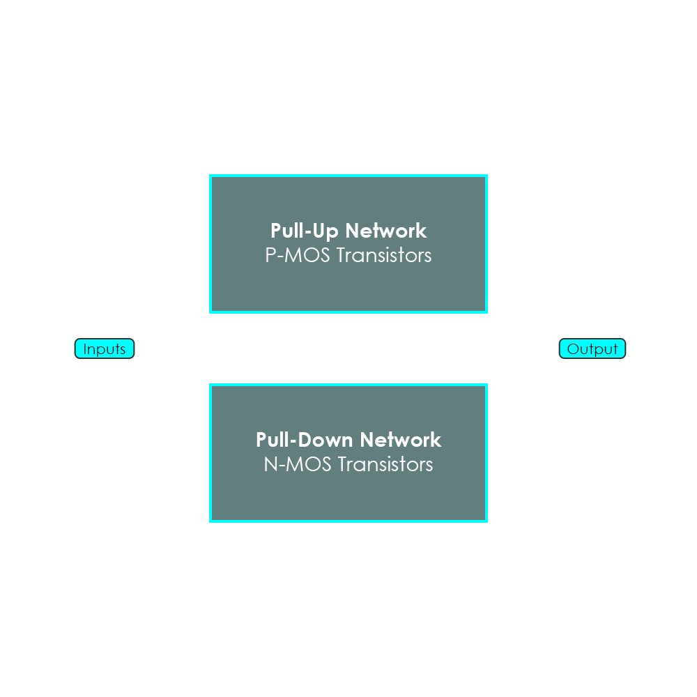
CMOS logic accomplishes this reduction in power consumption by using complementary pairs of P-MOS and N-MOS transistors. All P-MOS transistors must either be connected to the positive power rail or to another P-MOS transistor. Similarly, all N-MOS transistors must either be connected to ground or to another N-MOS transistor. A pair of complementary P-MOS and N-MOS transistors is connected to the same input signal. In this configuration, any signal will turn on a transistor of one type and off a transistor of the other type. This ensures that both transistors are never switched on at the same time.
The P-MOS transistors are typically connected to the positive power rail (VDD), and the N-MOS transistors are connected to ground (GND). When an output is tapped from the point between the P-MOS and N-MOS transistors, this output will either be directly connected to VDD (the P-MOS transistor pulls the output to high) or directly connected to ground (the N-MOS transistor pulls the output to low). For that reason, the P-MOS part of a CMOS circuit is also called the Pull-Up Network (PUN), whereas the N-MOS part of a CMOS circuit is called Pull-Down Network (PDN).
A high voltage on the input will cause the N-MOS to conduct and the P-MOS not to conduct. By contrast, a low voltage on the input causes the P-MOS to conduct and the N-MOS not to conduct. Both types of MOSFETs will conduct for a very short amount of time when switching, but not when keeping their state. This characteristic greatly reduces power dissipation, and therefore heat generation. The following illustrations show the circuits of the most common logic gates.
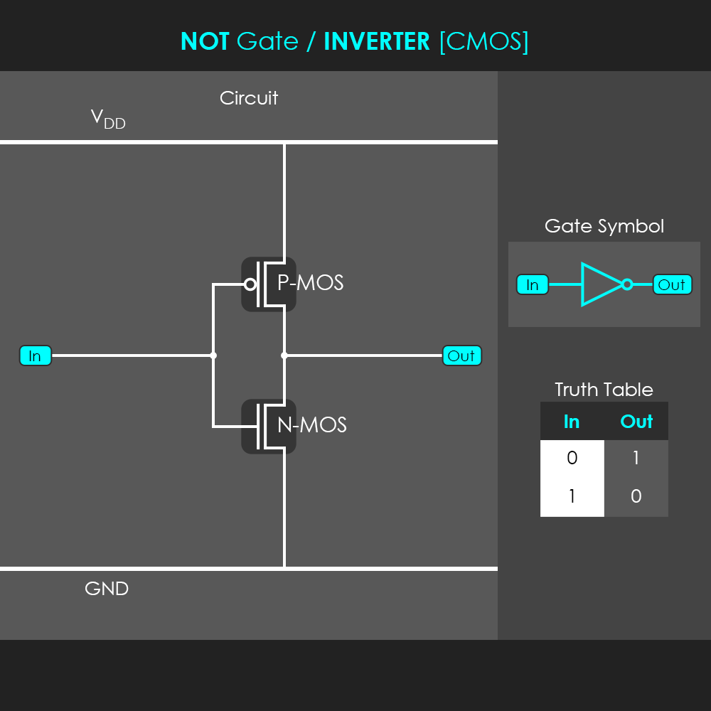
A CMOS inverter consists of two complementary transistors that are connected to the same input. When the input is low (0), the P-MOS transistor is conductive and acts like a closed switch, pulling the output to high (1). The complementary N-MOS transistor receives the same low input signal, and that causes the N-MOS to be non-conductive, disconnecting the output from ground. Vice versa, when the input is high (1), the P-MOS turns non-conductive, disconnecting the output from the positive power rail. This time the N-MOS transistor is conductive and acts like a closed switch, pulling the output to low (0). The circuit diagram shows very clearly how both P-MOS and N-MOS transistors complement each other to switch the output signals. The alternating operation also prevents any short circuits from occurring.
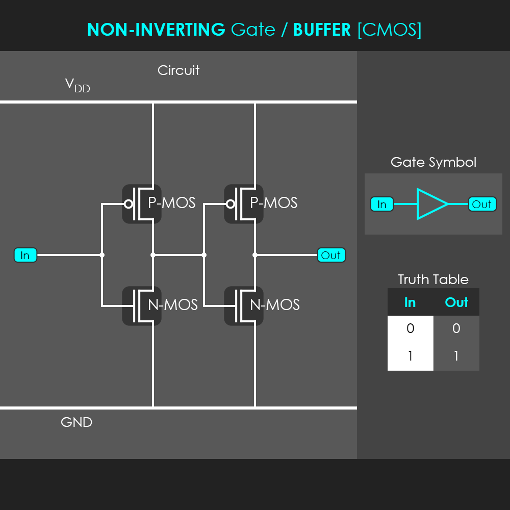
Similar to buffers from other logic families, a CMOS buffer is also created by a combination of two inverters in series. It is also very common for other CMOS gates to connect two stages of complementary logic in series.
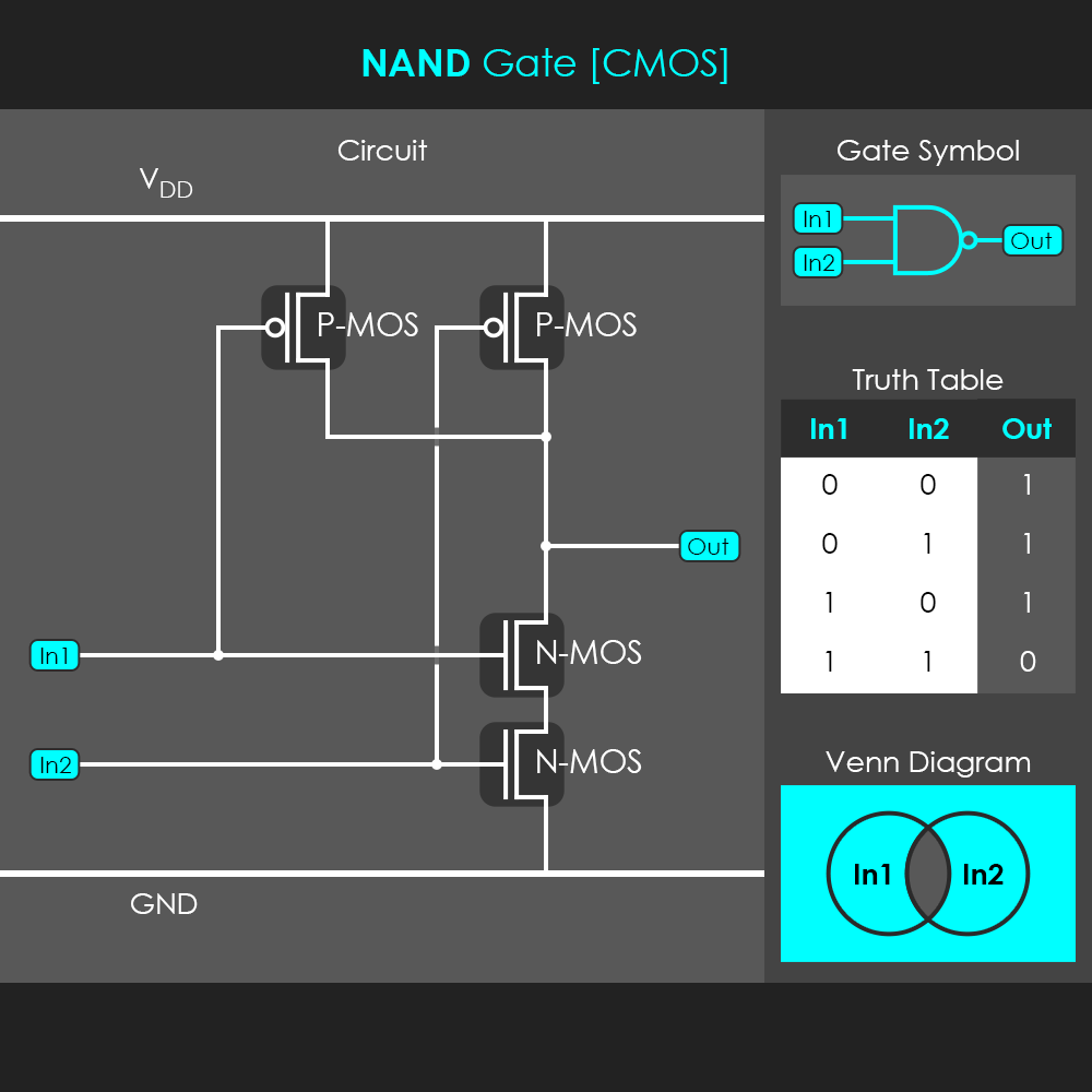
In a 2-input NAND gate, the pull-up network consists of two parallel P-MOS transistors with their source terminals connected to the supply voltage VDD. The pull-down network consists of two N-MOS transistors that are connected in series. The output is tapped at the point where the pull-up network and the pull-down network are linked together. Applying two high (1) input signals to the NAND gate turns both P-MOS transistors off, disconnecting the output from the positive supply rail. In addition, both N-MOS transistors are turned on by two high inputs, thus pulling the output to low (0). When one or both inputs are low (0), one or both P-MOS transistors are conductive, pulling the output to high (1). As both N-MOS transistors are arranged in series, having one or both input signals low always disconnects the entire pull-down network from ground. This shows that any low input signal turns the NAND gate on, but turns it off when both inputs are high. It is exactly the opposite of an AND gate.
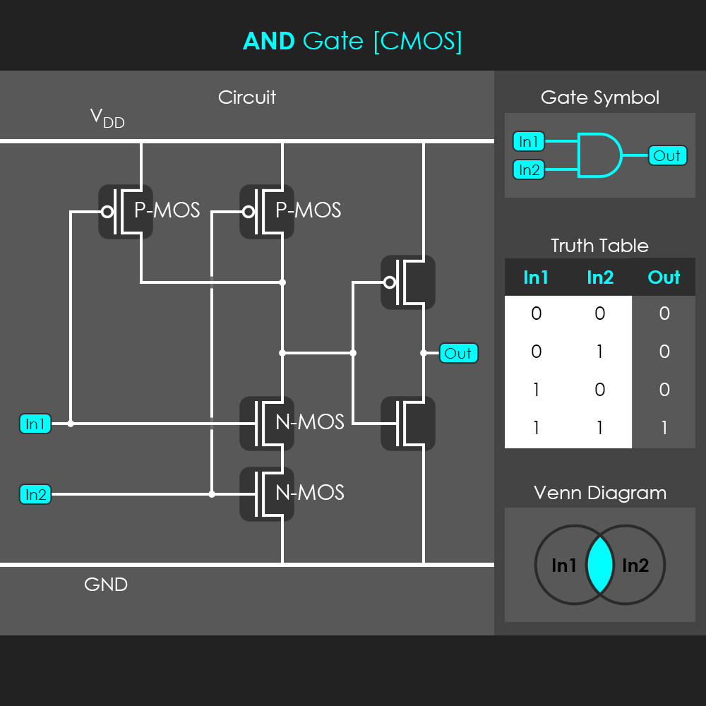
The 2-input AND gate is built from a NAND gate and an inverter. The NAND gate’s output is low only when both inputs are high, the inverter of the AND gate changes that logic. The AND gate’s output is high only when both inputs are high. For any other input combinations, the AND gate is low.
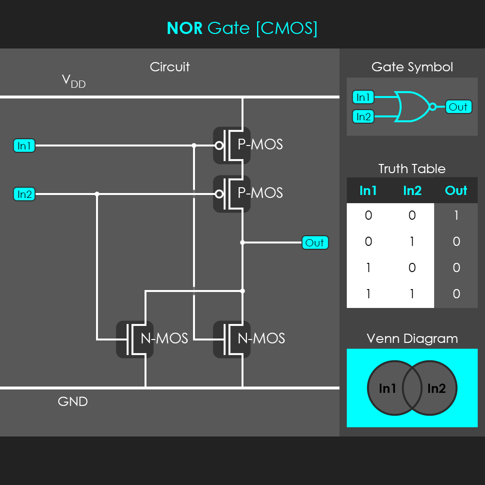
In a 2-input NOR gate, the pull-up network consists of two serial P-MOS transistors that are connected to the supply voltage VDD. The pull-down network consists of two parallel N-MOS transistors connected to ground. The output is tapped at the point where the pull-up network and the pull-down network are linked together. Having two low (0) input signals applied to the NOR gate is the only combination where both P-MOS transistors are turned on, pulling the output high (1). Any other situation with one or both of the inputs high (1) turns one or both P-MOS transistors off, disconnecting the output from VDD. One or both input signals high also turns one or both of the parallel N-MOS transistors on, directly pulling the output to low (0). It is exactly the opposite of an OR gate.
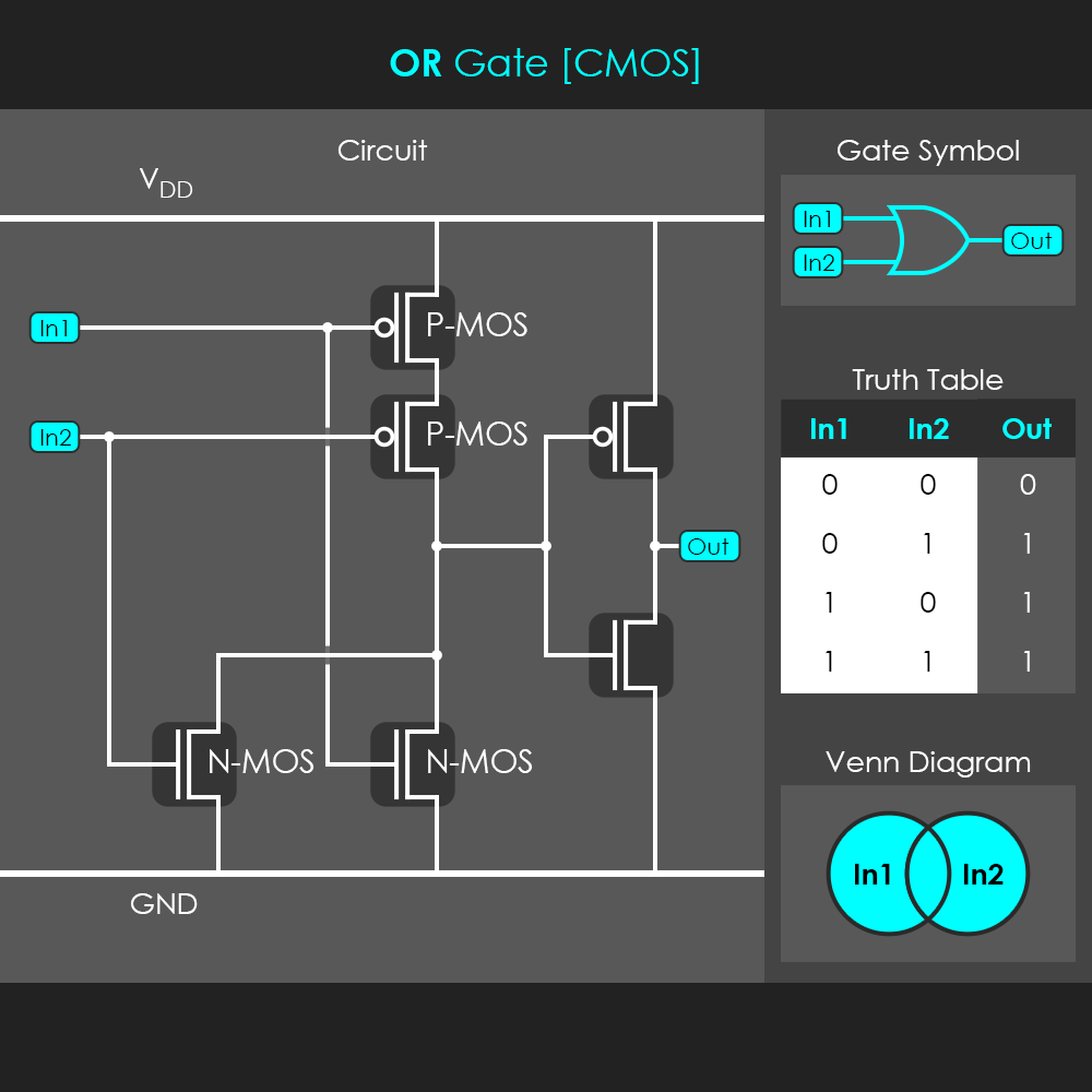
The 2-input OR gate is built from a NOR gate and an inverter. The NOR gate turns off when one or both inputs are high, and the inverter of the OR gate changes that logic. As soon as one of the inputs or both are high, the output of the OR gate is high.
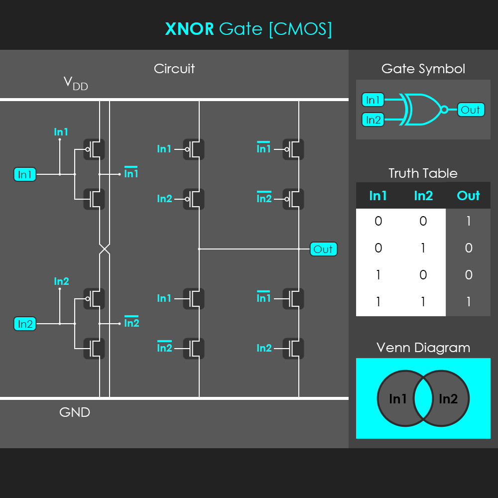
The circuit for the CMOS XNOR gate consists of twelve transistors, four of them are used to create two inverters. Each of the two input signals is fed into an inverter. With this setup, each input is split up into an original, non-inverted input signal and an inverted input signal, indicated with the overline above ‘In1′ and ‘In2′. Non-inverted and inverted In1 and In2 signals are applied to the P-MOS and N-MOS transistors as shown in the illustration. The output of an XNOR gate is only high when both inputs are identical.
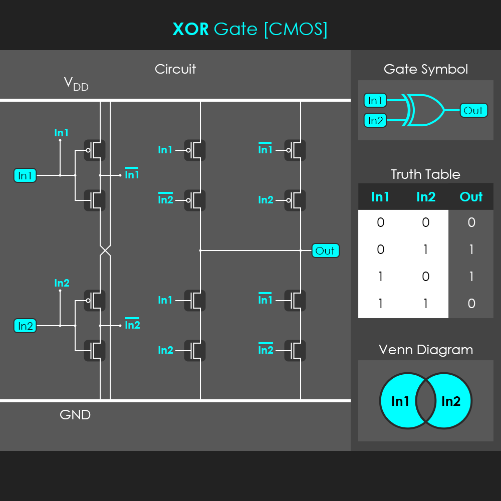
The circuit for the CMOS XOR gate is very similar to the one used for the XNOR gate. It splits up each of its input signals into non-inverted and inverted versions. The difference between the XNOR and the XOR gate is the way some of the transistors are connected to the input lines. The output of an XOR gate is only high when one input exclusively is high, having both inputs high turns the output of the XOR gate low.
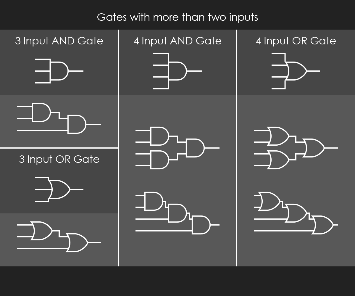
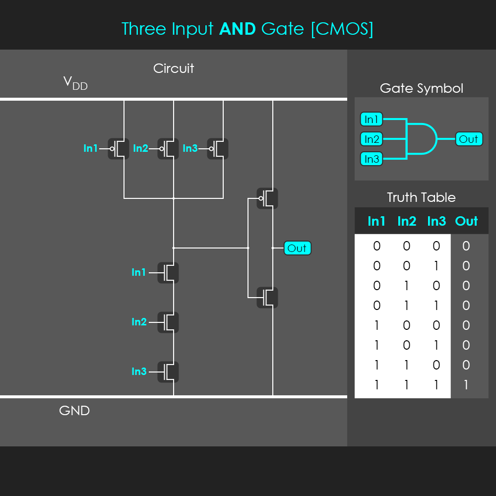
In integrated circuits, there are many applications that also use logic gates with more than two inputs. For instance, gates with three or four inputs are very popular among circuit designers. Those types of logic gates can be created by two different approaches: One possibility is to design an individual transistor circuit that precisely meets the requirements of the logic gate. This method is typically used when highly specialized logic gates need to be produced.
Another possibility to create logic gates with more than two inputs is to combine several two-input logic gates to a small network of gates that in total behaves like a larger gate with more than two input terminals. Both of these approaches are explained in further detail below.
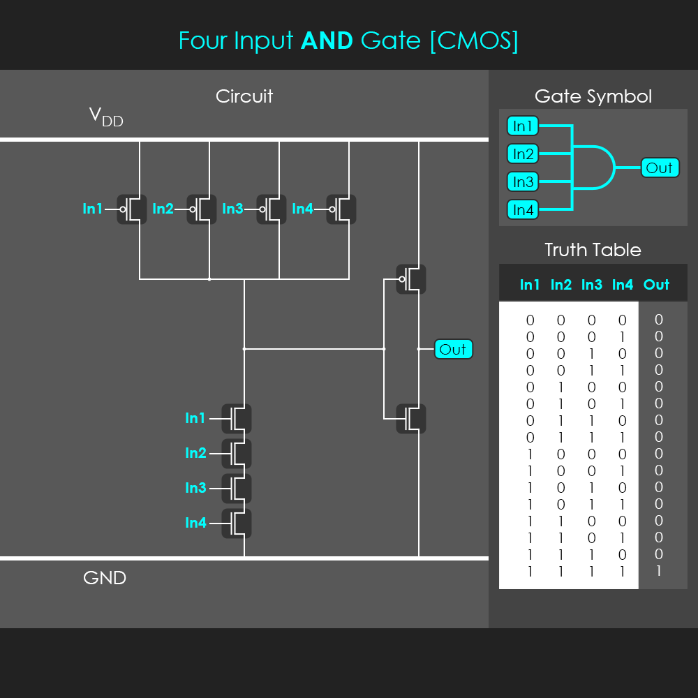
The illustrations below display three and four input AND gates built with CMOS circuits that are designed with three and four input lines. Having at least one input signal low does always keep one P-MOS transistor conductive and its complementary N-MOS transistor non-conductive. This in turn pulls the center point high, and the inverter changes that to a low output. Only if all inputs are high at the same time, the center point is pulled low, and the inverter changes that to a high output. Note that the basic structure (pull-up network with parallel P-MOS transistors, pull-down network with serial N-MOS transistors, and an inverter) is very similar to the two-inout AND gate.
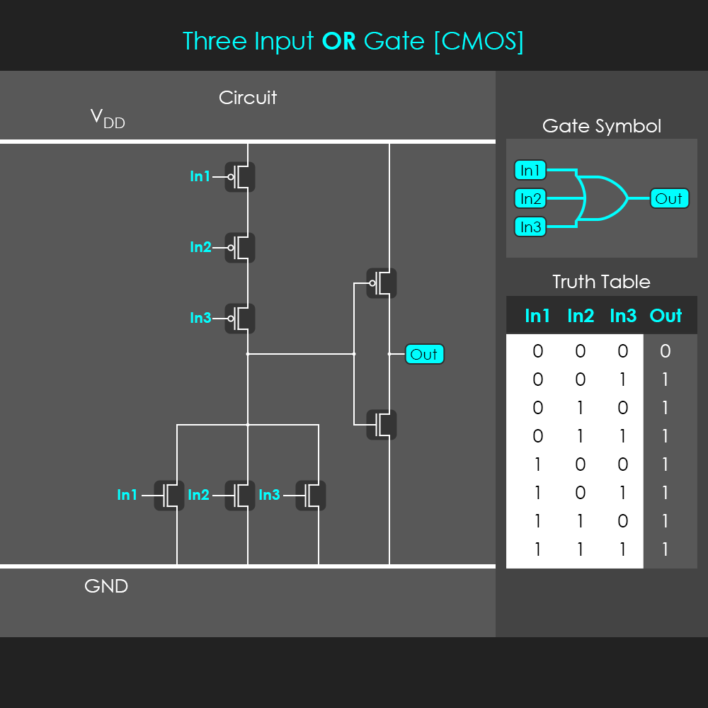
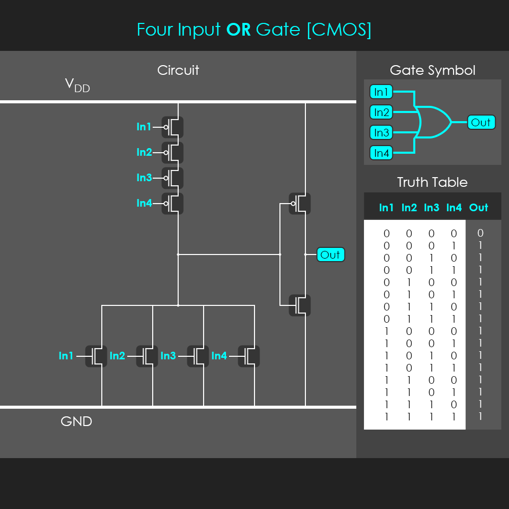
The illustrations below display three and four input OR gates built with CMOS circuits that are designed with three and four input lines. Having at least one input signal high does always turn one P-MOS transistor non-conductive and its complementary N-MOS transistor conductive. This in turn pulls the center point low, and the inverter changes that to a high output. Only if all inputs remain low at the same time, the center point is pulled high, and the inverter changes that to a low output. Note that the basic structure (pull-up network with serial P-MOS transistors, pull-down network with parallel N-MOS transistors, and an inverter) is very similar to the two-inout OR gate.
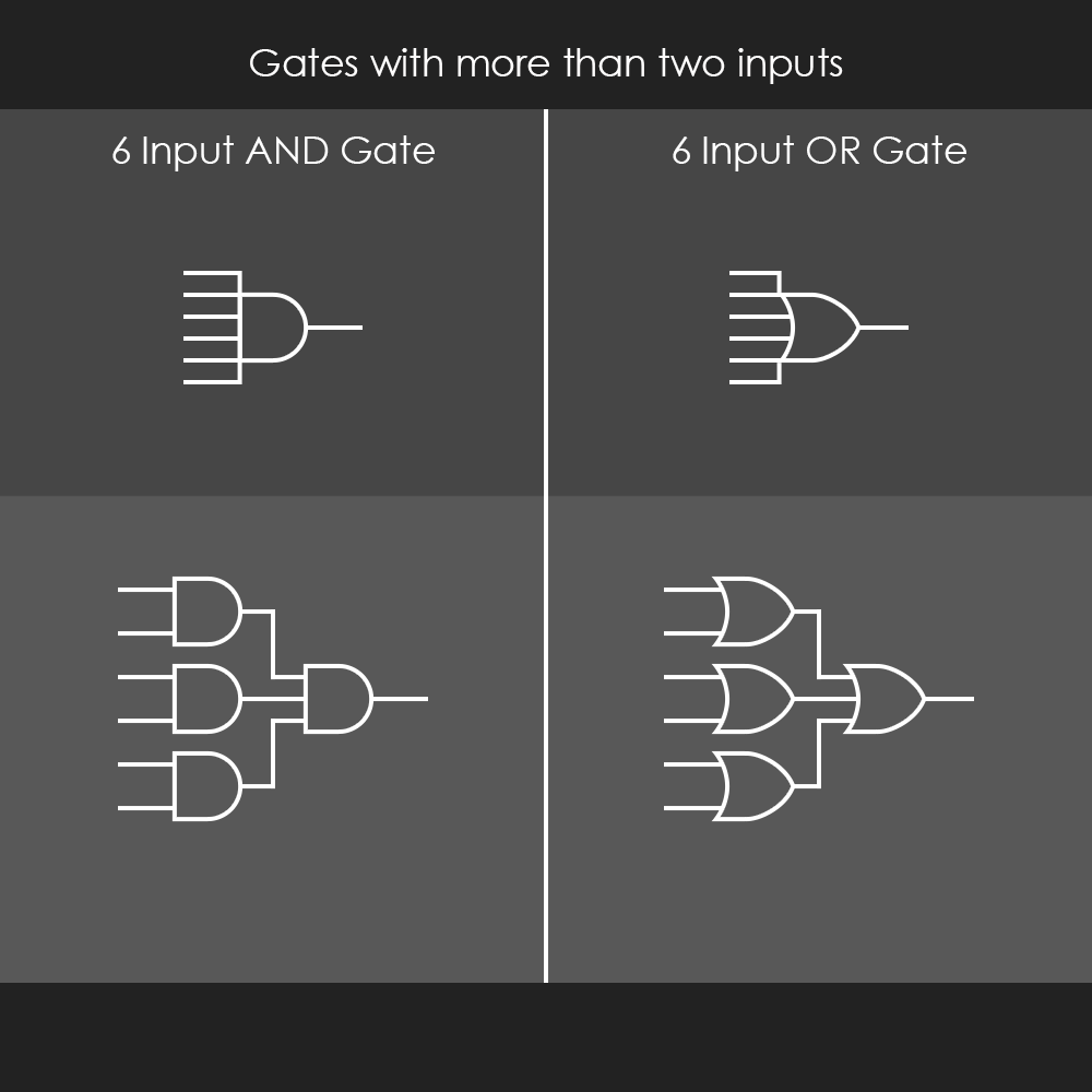
Unfortunately, having four P-MOS transistors chained in series can have some adverse effects on the operation of the gate. To ensure full performance and speed of a circuit it is desirable to avoid paths with many transistors connected in series. Another way to implement logic gates with more than two inputs is to combine several two-input gates to a small network of gates which in total behaves like a single gate.
The following illustrations show some approaches to create gates with more than two inputs by combining smaller gates. A three input AND gate can be created by connecting two AND gates so that the output from one AND gate feeds into one input of the other AND gate. A four input AND gate can be created by cascading two AND gates into another AND gate. Gates with even more inputs can be created in the same way.