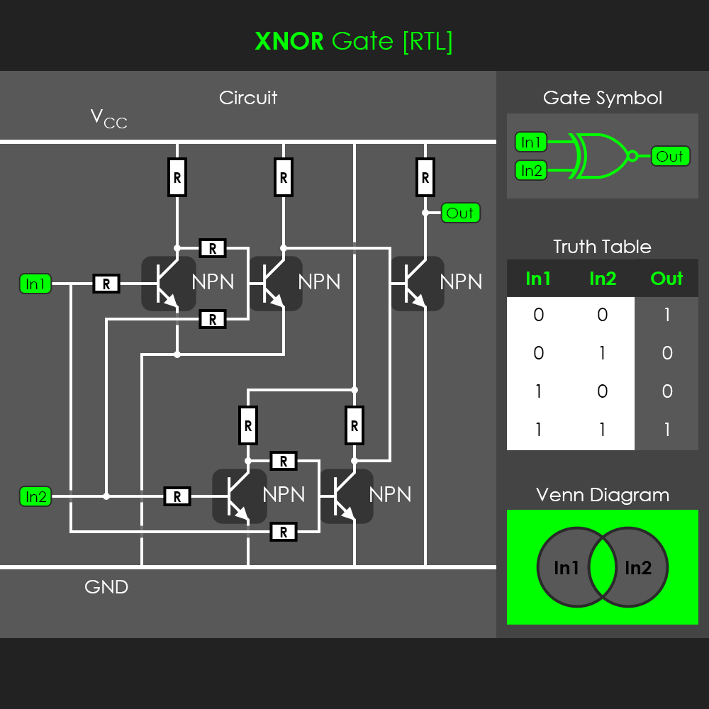
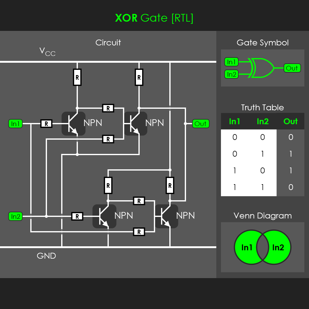
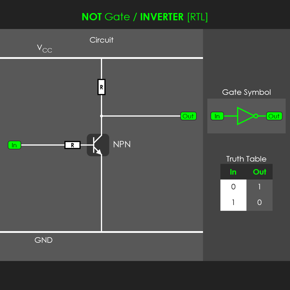
The Resistor Transistor Logic (RTL) is considered to be the first logic family that was introduced for integrated circuits. Logic gates that use RTL technology are designed using NPN transistors as switches and resistors as current limiters or to implement voltage drops. The following illustrations and explanations provide some further insight into the circuitry used to implement logic gates with RTL technology. Please note that the logic gates below are arranged in a different sequence as in the overview above. The illustrations are sorted by an increasing complexity of the circuits.
When the input is low (0), the NPN is in the off state, and acts like an open switch. In this state the output is disconnected from ground and connected to the VCC power supply through the resistor. As there is no current that flows between VCC and GND, there is also no current that flows through the vertical load resistor, which means that there is also no voltage drop across that resistor. For that reason, the output is pulled high (1). Only when the input is high (1), the NPN is in the on state, and acts like a closed switch, completing the circuit and establishing a current. Even though a current flows from VCC to GND, the output is now connected to the ground through the active NPN, and therefore pulled low (0). There is now a voltage drop occurring at the vertical resistor due to the current flowing through it.
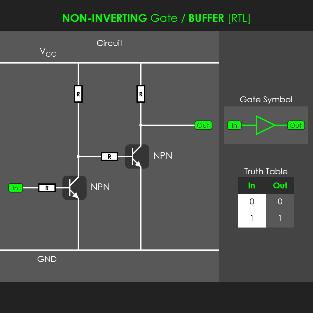
A buffer is technically two NOT gates (inverters) installed in series. Although the output is logically always the same as the input, the input signal itself cannot always be used for further signal processing. This is due to the fact that some input voltages may originate from other circuits where they have slightly dropped (for instance 11V instead of 12V) due to some voltage drop across prior components or due to other reasons. By using a buffer, even a slightly weaker input signal gets converted into a ‘new’ and stable output signal with full VCC voltage.
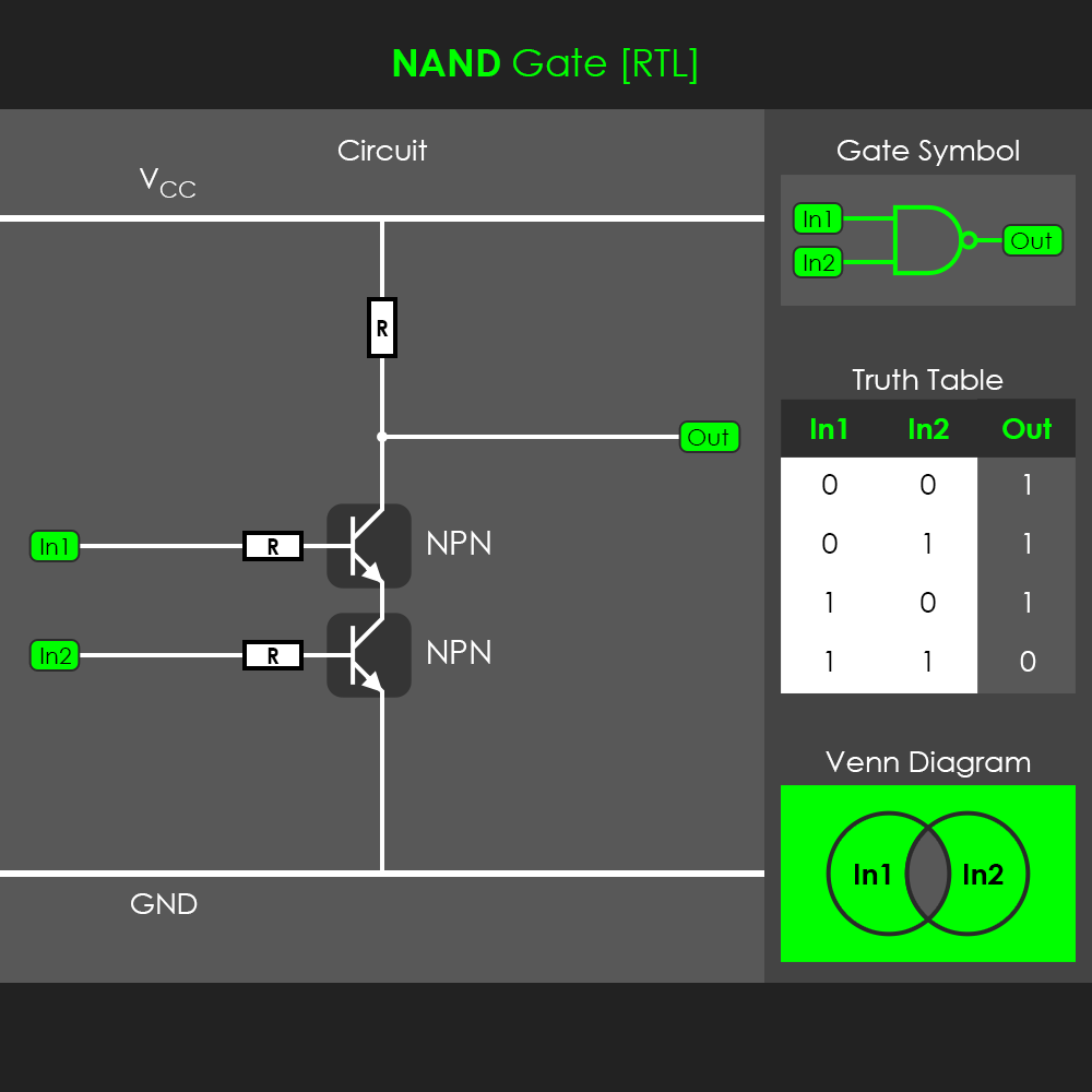
A NAND (Not-AND) gate is designed by two NPN transistors in series with a resistor. There are two input signals, each of them connected to the base of an NPN transistor. The output signal is taken from the indicated position. As long as both inputs are low (0), both NPNs remain in the off state and act like open switches. In this condition, the output is pulled high (1) as no current can flow in this circuit, and therefore no voltage drop occurs at the top resistor. Since both NPNs are connected in series, applying a high (1) signal to one of the inputs does not change anything either as there is still another transistor acting like an open switch. Only when both inputs are high (1) at the same time, both NPNs are in the on state, and act like closed switches, effectively connecting the output to ground. In this condition, the current induces a voltage drop at the top resistor, and the output is pulled low (0) due to the direct connection to ground.
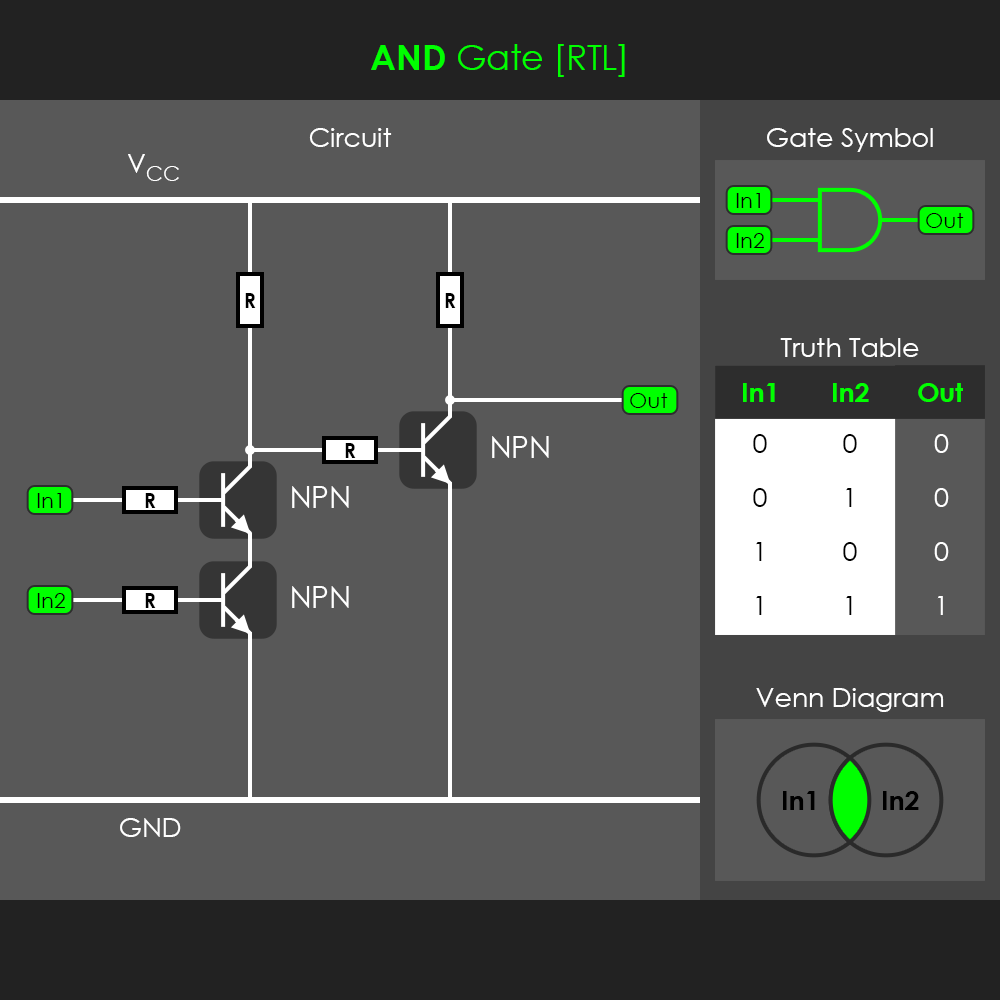
An AND gate is technically a NAND gate and a NOT gate (inverter) connected as shown in the image. In every condition where the NAND gate had a high (1) output (when both or either one of the inputs are low), the inverter turns this output into a low (0) output. Vice versa, the only condition where the NAND gate had a low (0) output (when both inputs were high), the inverter turns this output into a high (1). So the AND gate is only high when both NPNs are triggered by high inputs. This is also where the term comes from – input 1 AND input 2 have to be active in order to produce a high output signal on an AND gate.
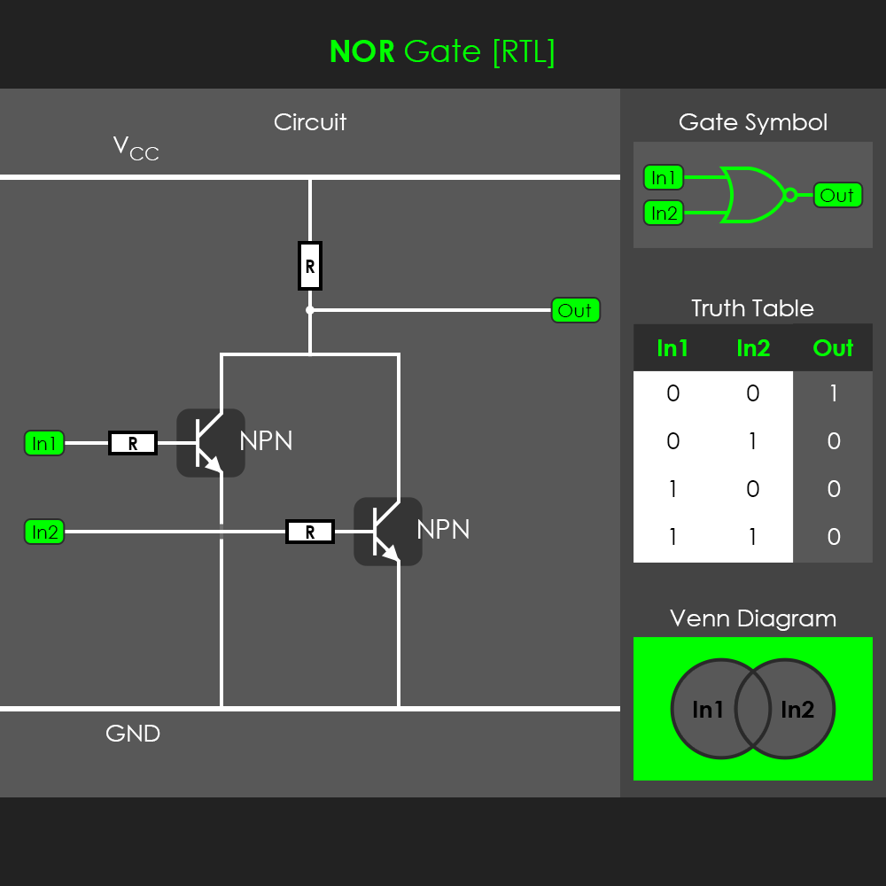
A NOR gate is created by two NPN transistors in parallel. There are two input lines, each of them connected to the base of one transistor. The output signal is taken from the indicated position. As long as both inputs are low (0), both NPNs remain in the off state and act like open switches. In this condition, the output is pulled high (1). This shows that the NOR gate behaves exactly like the NAND gate as long as both inputs are low. However, as soon as one of the inputs turns to high (1), one of the parallel NPNs activates, acting like a closed switch. Note that only one active NPN is sufficient to create a conductive path from VCC to GND. This connects the output to ground and pulls it low. Two high inputs at the same time have the same effect, they close the circuit and pull the output to low.
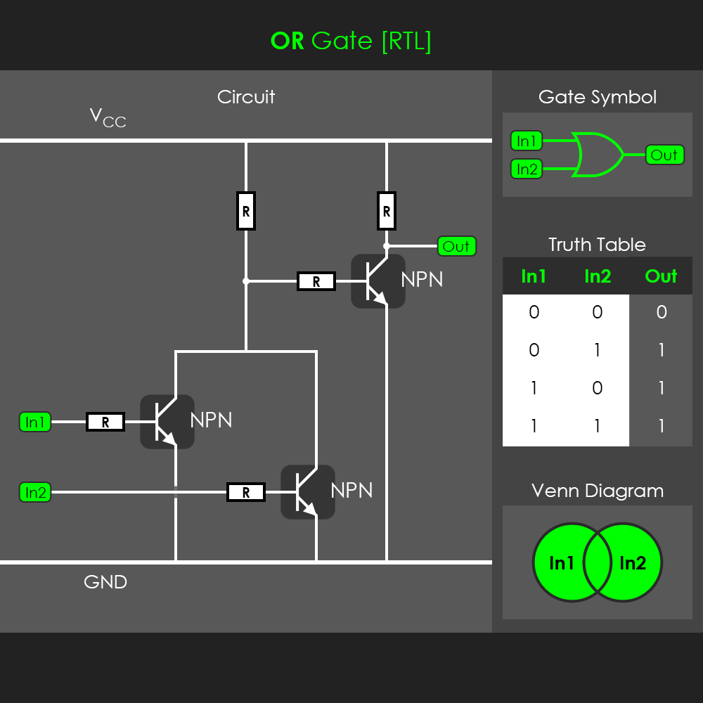
An OR gate is created by a combination of a NOR gate and a NOT gate (inverter). The inverter turns every output of the NOR gate into the opposite. This makes the OR gate stay low (0) whenever both inputs are low (0). As soon as one or both inputs turn to high (1), the NOR circuit is closed, connecting the base of the inverter to ground, causing the output to be pulled high (1).