While early cameras used photographic film to capture an image, today’s digital cameras rely on highly complex optoelectronic sensor arrays. This chapter presents various interesting functional principles and facts of modern image sensors and related optical elements.
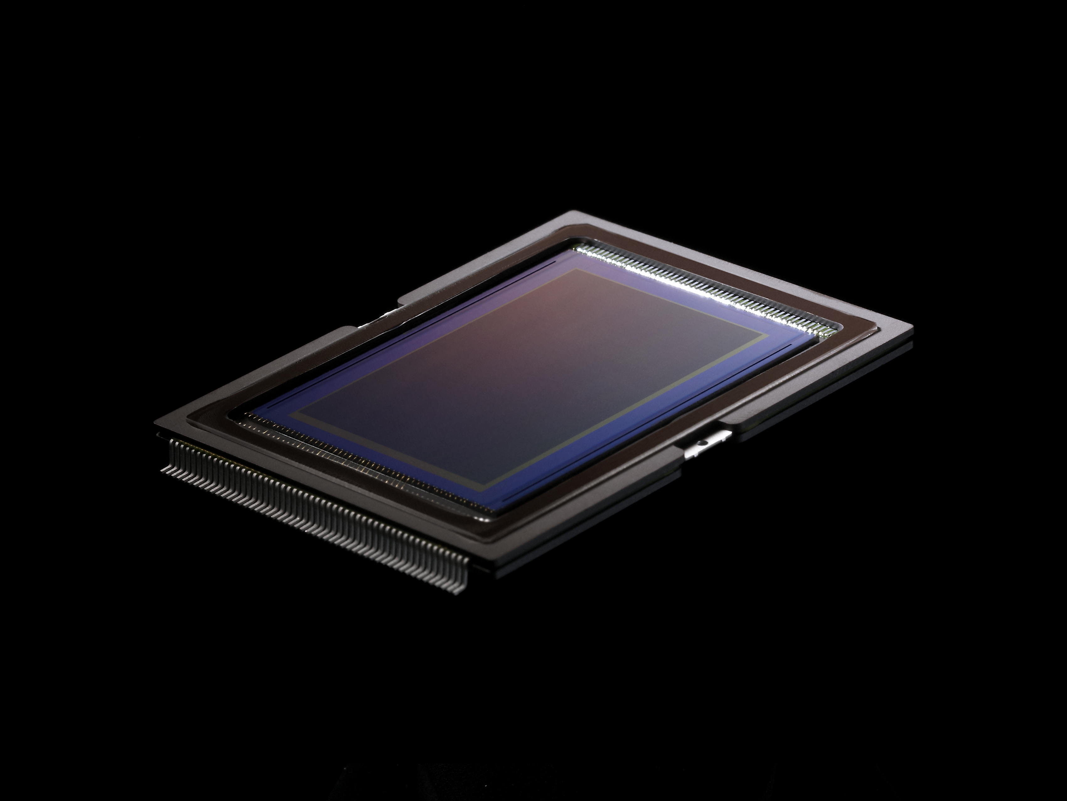
An image sensor is one of the core elements in a digital camera. Its performance is directly related to the quality and appearance of the photograph, including resolution, dynamic range, and color rendition. The image shows a sensor unit of a Canon EOS 1D X Mark II DSLR camera.
There are two major technologies used for digital image sensors: Charge-coupled devices (CCD) and CMOS sensors.
A charge coupled device in general is a circuit containing an array of certain capacitors that can transfer their electric charge to an adjacent capacitor. In an image sensor that uses charge-coupled device technology, the capacitors are the primary units that are used to create light-sensitive pixels. In these capacitors photons are converted into electric charges that build up in the semiconductor, and that can be read out by the camera. The readout of a CCD image sensor typically begins with the lowest line of pixels that transfers their charges (one after another) to an electron-to-voltage converter where charges are evaluated and downstream electronics can begin to store one line of the image. Once all charges from the lowest line of pixels have been read out, the next line of pixels transfers its charges to the lowest line of pixels. The lowest line can again transfer all charges to the converter. This process continues until the entire CCD image sensor has been read out, and until a complete image has been stored by the camera. It is important to understand that CCD image sensors do not require additional readout circuitry embedded into the pixels, because the specialized light-sensitive capacitors are able to transfer their charges to the neighboring pixels without the requirement for any active components. CCD image sensors have been invented in the 1960 and they are still widely used today. Due to their higher production cost, they are mainly used for industrial, medical and scientific imaging equipment as well as for high end video cameras.
A CMOS sensor uses an approach where photodiodes are directly integrated into a more complex readout structure. Every pixel of a CMOS sensor has one or more transistors integrated. The semiconductor technique used for the transistors is called complementary metal-oxide semiconductor (CMOS), hence the name of the sensor technology. The transistors in each pixel are used for readout activation, signal amplification, or noise reduction. CMOS sensors are most commonly used in today's smart devices and digital cameras. They offer good image performance, high readout speed and low power consumption. CMOS image sensors can be produced with similar semiconductor processes as microchips, which makes this type of image sensor very cost effective.
There are two types of pixel configurations in CMOS technology: active and passive. An active pixel requires a photodiode and a minimum of three transistors to process the signal. In contrast, a passive pixel consists of a photodiode with a single transistor.
Passive-pixel sensors (PPS) were the first image-sensor devices used in the 1960s. A passive-pixel sensor consists of pixel units which are read out without amplification or noise reduction, with each pixel consisting of a photodiode and one transistor. The photodiode converts incident photons into an electrical charge. This charge is then read out and amplified by external circuitry. While passive pixels can be built very small and offer a higher fill factor due to their limited on-pixel circuitry, they are more likely to suffer from noise.
An active-pixel sensor (APS) consists of pixels that have one or more transistors integrated to amplify the photodiode's signal, to convert the photo-generated charge into a voltage, and to reduce noise. In order to reduce noise effectively, active pixels often determine what the noise level is in the dark, and they subtract that dark noise level from the final signal generated by the photodiode. It is this active circuitry that gives the active-pixel sensor its name. Therefore an active-pixel sensor combines both the image capturing function and image processing functions within the same integrated circuit. APS sensors have shown to be superior to passive pixel sensors. However, due to an increased area used for circuitry, active-pixel sensors offer a lower fill factor. Active pixel sensors are the most common type of CMOS sensors for consumer goods such as smartphones, tablets, notebooks, and DSLR cameras. This chapter on image sensors focuses on active-pixel CMOS sensors.
The fill factor of an image sensor is the ratio of a pixel's light sensitive area to its total area, and it is expressed in a percentage. CCD sensors usually have a fill factor of around 100% whereas CMOS sensors offer much less. For that reason, CMOS sensors typically have an array of microlenses applied on top of the light sensitive area, one microlens for each pixel. The purpose of these microlenses is to gather light from the non-sensitive circuitry areas of the pixel and focus it into the photodiode. This increases the effective fill factor of an active pixel sensor because less light actually hits the non-sensitive circuitry.

There are numerous different designs of image sensors. One differentiating factor of camera sensors is the size of the light sensitive area. The diagram compares some of the most common image sensor formats. sensors with a format smaller than 2/3″ are normally used for smart devices while larger formats are typically used for dedicated photographic equipment. Some special film cameras like the ones used for IMAX films even use 70mm sensor formats (70mm x 48,5mm) which is almost twice the size of a medium format sensor. The full frame format plays a special role in photography as the surface area of a full frame sensor corresponds to the ensitive area of traditional photographic film.
When camera sensor designers specify the size of an image sensor, they have to find a very good balance between a high pixel count and a high pixel size. While a high pixel count is desirable to achieve high resolution images, a high pixel size is useful to achieve better dynamic range and to reduce noise. However, both properties cannot be maximized at the same time, as they are adversely correlated with each other. In addition, the size of the image sensor affects the depth of field in the photograph. For a given lens aperture, an increased sensor size decreases the depth of field between the foreground and background. A shallow depth of field is often desired by photographers as it isolates the subject from the soft background.
An image sensor performs a conversion from light to an electrical signal. In order to record a complete image of the photographic scene, the sensor needs a large number of tiny receptors, called pixel sensors. A pixel sensor consists of some supply structures such as silicon substrate, some supply electronics (mostly ultra-thin metal wires) and a photosensitive area. The light sensitive area usually consists of a photodiode and is usually smaller than the total pixel area. A photodiode is a semiconductor with a very special characteristic that allows it to detect incoming light. A photodiode typically consists of silicon as this material has some very favourable properties.
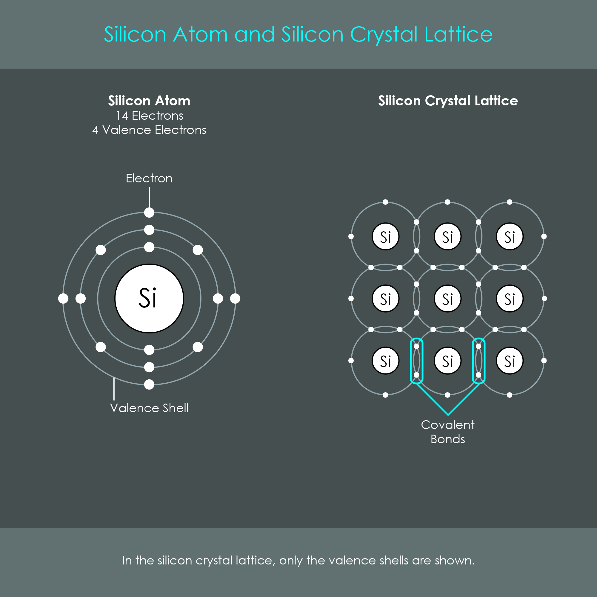
A single silicon atom consists of a nucleus of 14 positively charged protons and 14 (electronically neutral) neutrons surrounded by 14 negatively charged electrons. Each atom has various electron shells – depending on the number of electrons – where the inner shells always contain fewer electrons and the outer shells have a larger capacity for electrons. The formula to calculate the maximum electron capacity for a particular shell is 2n² where n is the number of the electron shell, beginning with 1 at the innermost shell. This results in a 2, 8, 4 layout for silicon while the outermost shell – called valence shell – could theoretically contain up to 18 electrons but the silicon atom simply does not have more than four electrons left. The silicon atom itself does not have an electric charge as there is an equal number of positive and negative charges (14 protons and 14 electrons). Of the 14 electrons, only the four outer electrons – called valence electrons – are available for chemical bonding. The remaining 10 electrons do not form bonds to other atoms due to their tighter adhesion to the nucleus. For this reason, each silicon atom can bond to four other silicon atoms. Such a chemical bond consists of two electrons as one electron from each of the silicon atoms is involved in the bond. When electrons are shared equally by the atoms involved, this type of connection is called covalent bond.
This structure of a silicon atom with four valence electrons gives silicon a very nice property: It can form a crystal using all of its valence electrons for bonding with a neighboring atom so that no valence electron is left over. This formation is very hard to break and creates an extremely stable crystal lattice. The silicon crystal that is formed has no electric charge as the silicon atoms themselves have no electric charge (having the same number of electrons as protons). The illustration depicts the structure of a single silicon atom and the formation of a silicon crystal lattice.
Applying a procedure called doping, the silicon’s pure crystal structure is intentionally changed by impuritiy atoms to modulate it’s electric characteristics. By a highly complex chemical procedure not further explained here, two types of doped silicon material are created. Negatively doped (n-type) silicon features an additional electron inbetween the atom bonds. The name n-type results from the negative charge of electrons. Positively doped (p-type) silicon features a missing electron between two silicon atoms, called hole. The following descriptions explain in detail what the doping procedure does to the silicon structure.
Just like the silicon atom, a single phosphorus atom has no electric charge by itself as the number of protons and neutrons is balanced. Phosphorus has 15 electrons and 15 protons. The doping procedure replaces some of the silicon atoms in the crystal with phosphorus atoms, called dopants. These dopant phosphorus atoms also create four covalent bonds with their neighbors in the same way as a silicon atom does. There is however a fifth valence electron in phosphorus that cannot be used for covalent bonding. This excess electron now plays an important role. This last valence electron is so weakly attached to the phosphorus atom that at normal temperatures the thermal energy within the crystal is sufficient to free it from the phosphorus atom. This results in an untethered electron that is free to travel around the crystal. When an atom with more than four bonding electrons is used to dope silicon, the dopant is also called a donor atom or donor impurity. The resulting crystal material is called n-type silicon as the free electrons available from the donor atoms each have a negative electric charge.
A boron atom has five protons and five electrons. With this property it can also be used for doping a silicon crystal where a silicon atom is replaced by a boron atom. As a boron atom has only three electrons available in its valence shell, only three covalent bonds can be established between a boron atom and the silicon atoms in a crystal. At normal temperature, there is sufficient thermal energy to push a nearby electron into this vacancy. If this is the case, the atom that supplied the electron to the boron atom now has an electron vacancy that can be filled by an electron from another atom in the crystal. In this way, the vacancy (also called hole) can move from atom to atom. This can be viewed as positive charges moving through the material as moving holes. When an atom with fewer bonding electrons than silicon is used to dope silicon, the dopant is also called acceptor atom or acceptor impurity. The resulting material is called p-type silicon as these types of dopant atoms generate mobile holes in the crystal with each hole having a positive electric charge.
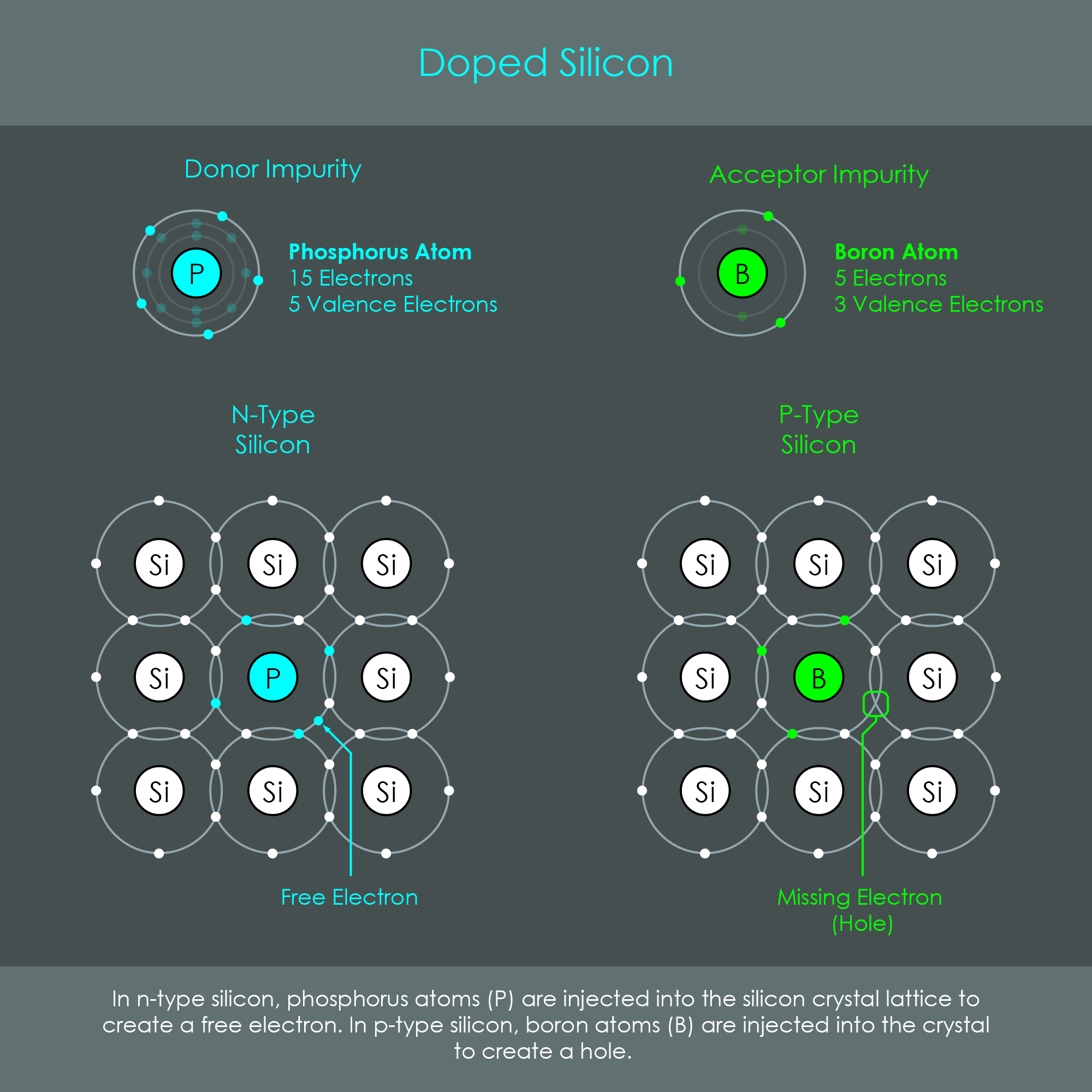
The image shows both types of doped silicon including the different impurity atoms. In an n-type phosphorus doped silicon crystal the free electrons will diffuse throughout the crystal in a purely random fashion until there is an equal distribution of free electrons throughout the volume of the n-type silicon crystal. In a p-type boron doped silicon crystal the corresponding holes will become equally distributed throughout the p-type crystal’s volume.
Doping one side of a piece of silicon with boron (a p-type dopant) and the other side with phosphorus (an n-type dopant) forms a p-n junction. The n-type material has large numbers of free electrons that can move through the material, but there are no free electrons on the p-type side. The p-type material has large numbers of holes that can move through the material, but there are no holes on the n-type side. These concentration gradients create diffusion forces on both electrons and holes. Electrons and holes start to diffuse to the opposite sides.
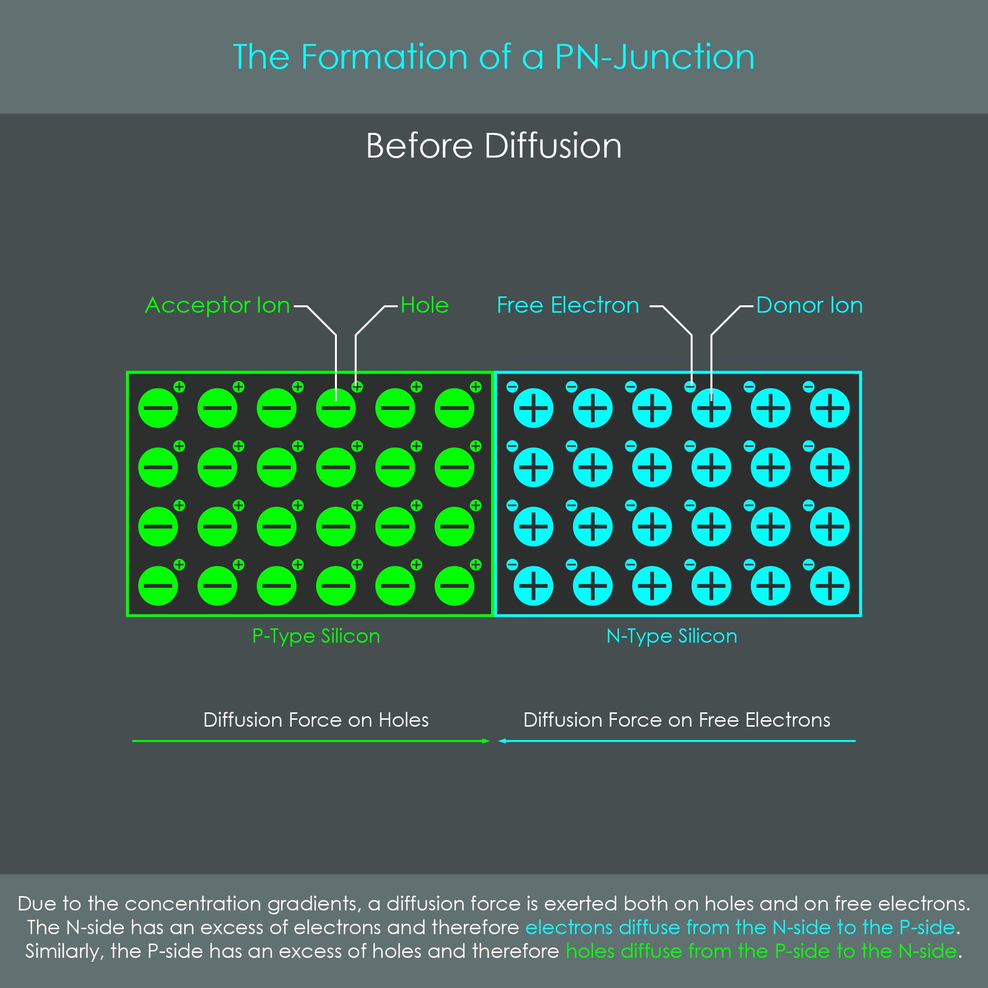
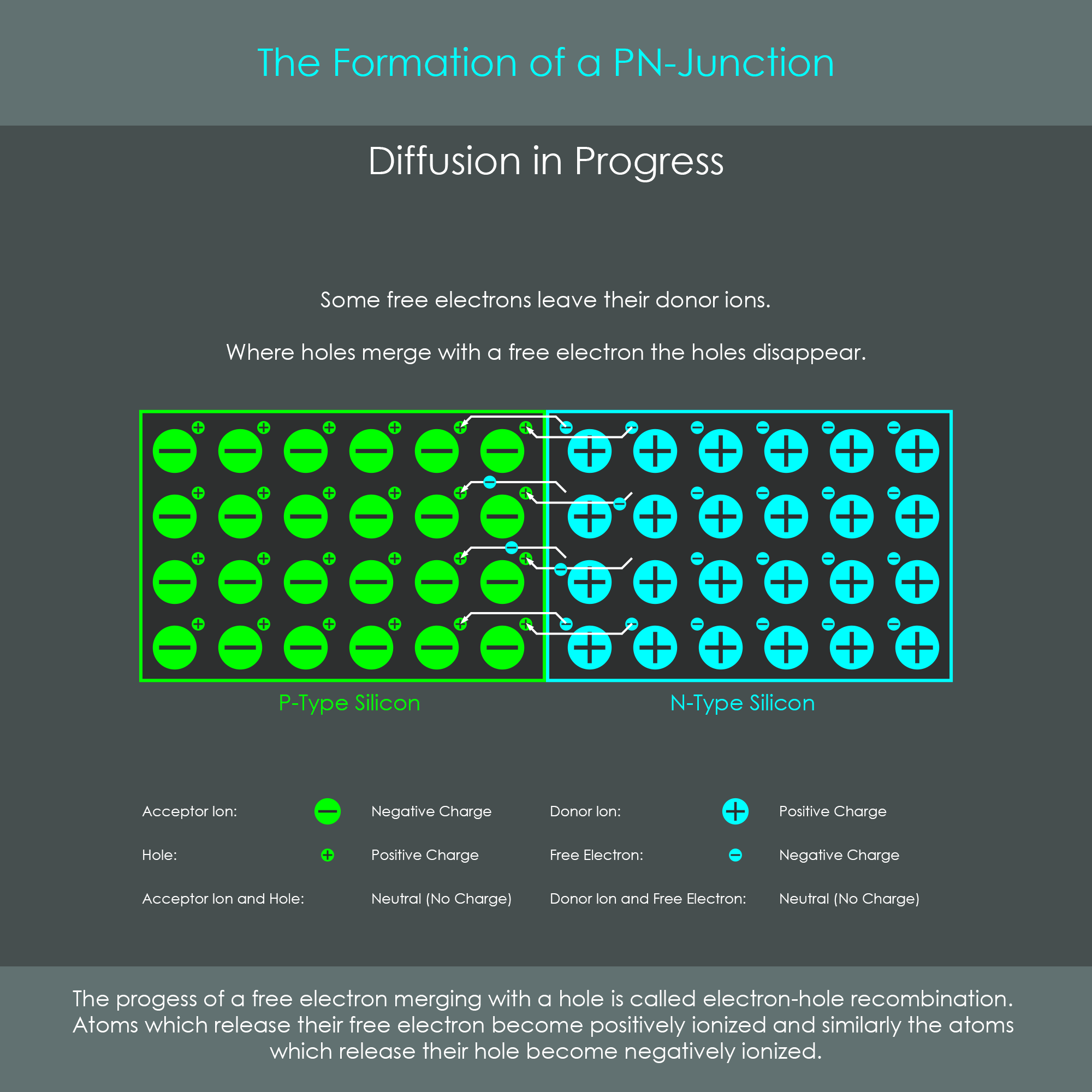
During diffusion, some free electrons leave their atoms and merge with a hole on the other side. This diffusion, however, does not allow all free electrons to recombine with all holes from the p-type side. As the electrons in the n-type material diffuse onto the p-type side, they leave behind positively charged phosphorus ions in the region where n-type silicon is close to the p-type side. Where holes merge with a free electron the holes disappear, and they leave behind a negatively charged boron ion. (The disappearance of a hole can also be seen as a hole diffusing onto the n-type side as a positive charge was moved from the p-type side to the n-type side.)
The charged ions now establish an electric field that repels further free electrons (and holes) from diffusing.
The formation of an electric field is what slows down and eventually stops any further movement of free electrons and holes. The diagram shows the direction of the electric field and how it exerts forces on electrons and holes. There will ultimately be an equilibrium between the diffusion forces from both sides, and the repelling force of the built-in electric field. This equilibrium forms a region where no free electrons and no holes remain. This zone is called the depletion region, and this region plays an important role in the detection of light.
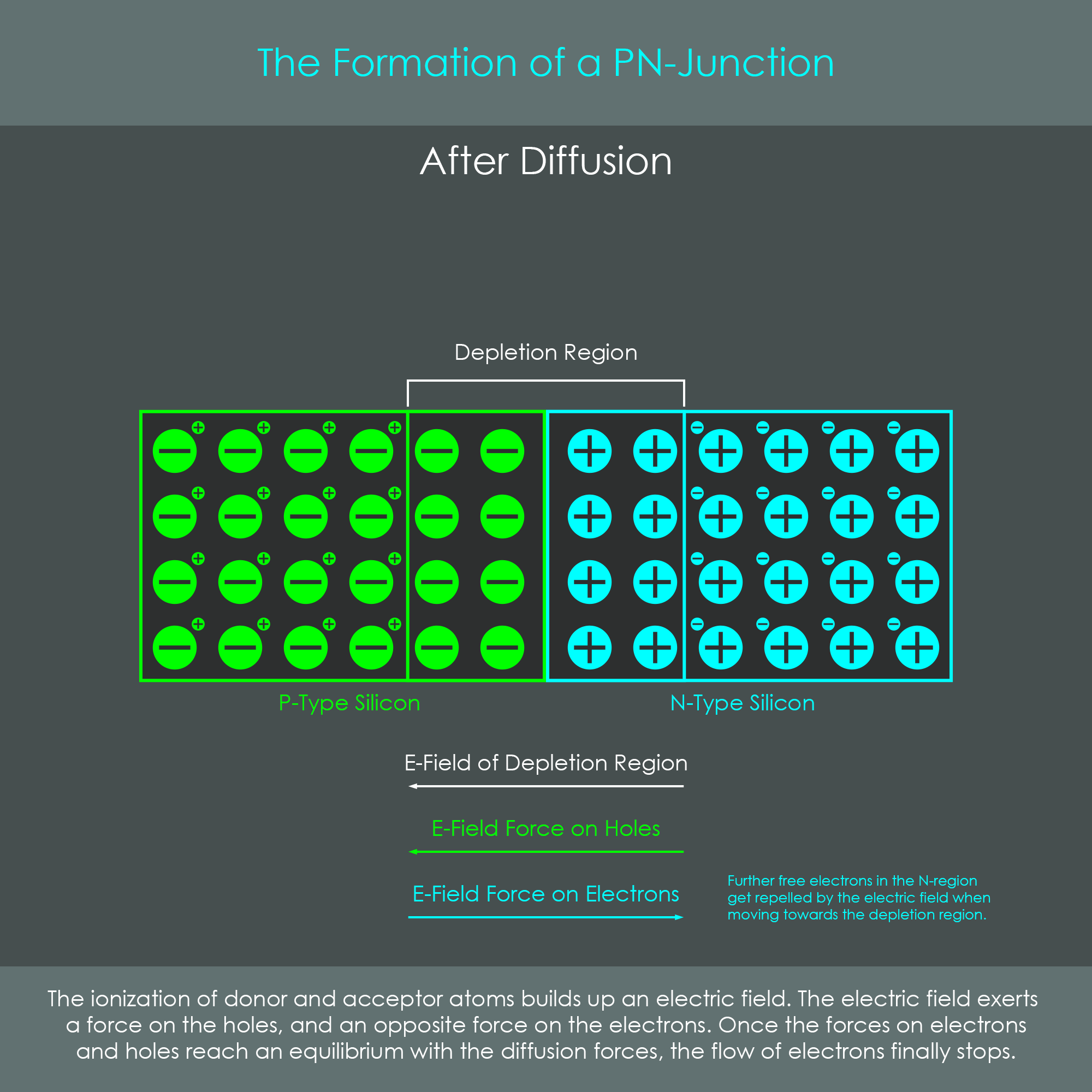
Within the depletion region, there are no free electrons and holes. It is therefore 'depleted' of mobile charges, leaving only the fixed charges originating from the ionized atoms. As a result, the depletion region is highly resistive and now behaves as if it was pure crystalline silicon: Like a strong insulator. The resistance of the depletion region can be modified by 'adding' an external electric field to the built-in electric field. If the added electric field has the same direction as the built-in electric field, the depletion region’s resistance will become even stronger. If the added electric field is opposite to the direction of the built-in electric field, the depletion region’s resistance will become smaller. The depletion region can therefore be considered a voltage-controlled resistor. This is the fundamental operating principle of a diode, that allows current to flow when a voltage of a certain polarity is applied (forward bias), and blocks all current from flowing when the voltage is applied in an opposite polarity (reverse bias).

If a positive voltage is applied to the p-type side and a negative voltage to the n-type side, current can flow (depending upon the magnitude of the applied voltage). This configuration is called forward bias. At the p-n junction, the built-in electric field and the applied electric field are in opposite directions. When these two fields overlay, the resultant electric field is smaller than the original built-in electric field. This results in a thinner, less resistive depletion region. If the applied voltage is large enough, the depletion region’s resistance becomes negligible. In silicon, this occurs at about 0.6 volts forward bias. From 0 to 0.6 volts, there is still considerable resistance due to the depletion region. Above 0.6 volts, the depletion region’s resistance is very small and current flows virtually unimpeded. The flow of current builds up because in the narrow depletion region, free electrons are not longer rejected by a strong electric field. The negative terminal of the battery keeps pushing new electrons into the n-type silicon, and the positive terminal of the battery keeps removing electrons from the p-type silicon (which is similar to adding holes to the p-type side). In the narrow p-n junction, new electrons and new holes constantly recombine, establishing a current.
If a negative voltage is applied to the p-type side and a positive voltage to the n-type side, no current is allowed to flow. This configuration is called reverse bias. At the p-n junction, the built-in electric field and the applied electric field are in the same direction. When these two fields overlay, the resultant electric field is much larger than the built-in electric field, and goes in the same direction. This creates a wider, more resistive depletion region. If the applied voltage becomes larger, the depletion region becomes even wider and more resistive. In reality, some current will still flow through this resistance, but the resistance is so high that the current may be considered to be zero. As the applied reverse bias voltage becomes larger, the current flow will saturate at a constant but very small value. The concept of silicon doping as well as the bias modes are key elements for the functioning of diodes.

When a diode is used for light detection, it is called a photodiode. For a photodiode to be able to detect light, it has to be driven in reverse bias mode. The goal is to prevent a current from flowing through the device. When an incident particle of light (photon) hits the depletion region, an electron is knocked out of its position, creating an electron-hole-pair. The electron is attracted towards the n-type layer by the electric field, the hole is attracted towards the p-type. It is the flowing electron that creates a small current that can be registered by the readout circuit. Depending on the sensor design, some current-to-voltage conversion is usually applied during the readout process. More details on readout electronics can be found on the signal processing chapter.
There is a proportional relationship between the intensity of incoming light (number of photons) and current flowing in the photodiode. While low light only produces a small current, bright light generates higher currents. Nevertheless, standard photodiode designs have a slight disadvantage when it comes to light detection: The knocked-on electron can only create a current when it is accellerated in the depletion region. A photon knocking out an electron in either the p-type or n-type side of the diode will also create an electron-hole-pair, however these will quickly reunite as there is no electric field effecting them. As the depletion region typically is much smaller than the entire semiconductor, the quantum efficiency of this regular design is quite low. For that reason, image sensors typically use PIN photodiodes to improve quantum efficiency.
The fundamental principle of a PIN photodiode is similar to the standard photodiode that uses a p-n-junction. However, instead of placing the p-type and n-type sides directly together to create a depletion region, an intrinsic layer is placed between the two doped layers. An intrinsic layer is not doped (or very lightly n-doped) and is therefore highly resistive. Due to that resistance, an intrinsic layer also increases the electric field strength in the photodiode. This greatly increases the volume of the depletion region, and therefore increases the volume for photons to hit and be converted to electric current. A PIN photodiode is usually oriented in a way so that n-type, intrinsic, and p-type layers are stacked vertically above each other. In this configuration, the photodiode's intrinsic layer has a larger area oriented towards incoming photons. Another improvement is made by developing the top layer as thin as possible (~1μm). The intrinsic layer is usually ~4-6μm thick. All these advantages and improvements give PIN photodiodes a higher quantum efficiency than p-n-junction photodiodes. The illustration below shows a cross-section through a PIN photodiode as they are used in modern image sensors.
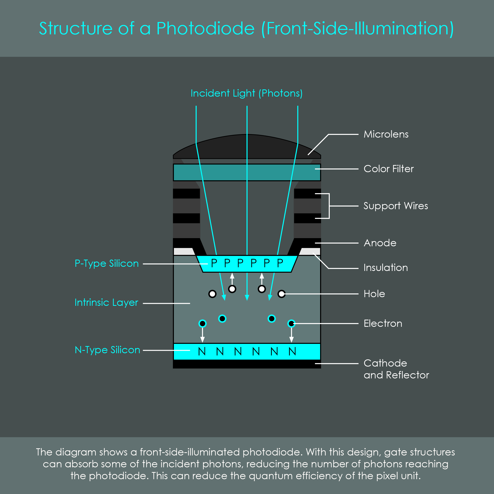
As described, the surface of a sensor pixel is not completely sensitive to light but rather features a smaller zone (also called photosite) where the photodiode is placed. The remaining part of the pixel is used for supply and readout electronics. With this design given, a large proportion of the incoming light would actually illuminate the non-sensitive areas with the pixel unable to convert all photons into light. To improve the quantum efficiency even more, little micro lenses are typically placed on top of the pixels to direct as many photons into the active photodiode as possible. Some sensor designs even use two layers of microlenses to minimize the loss of photons.
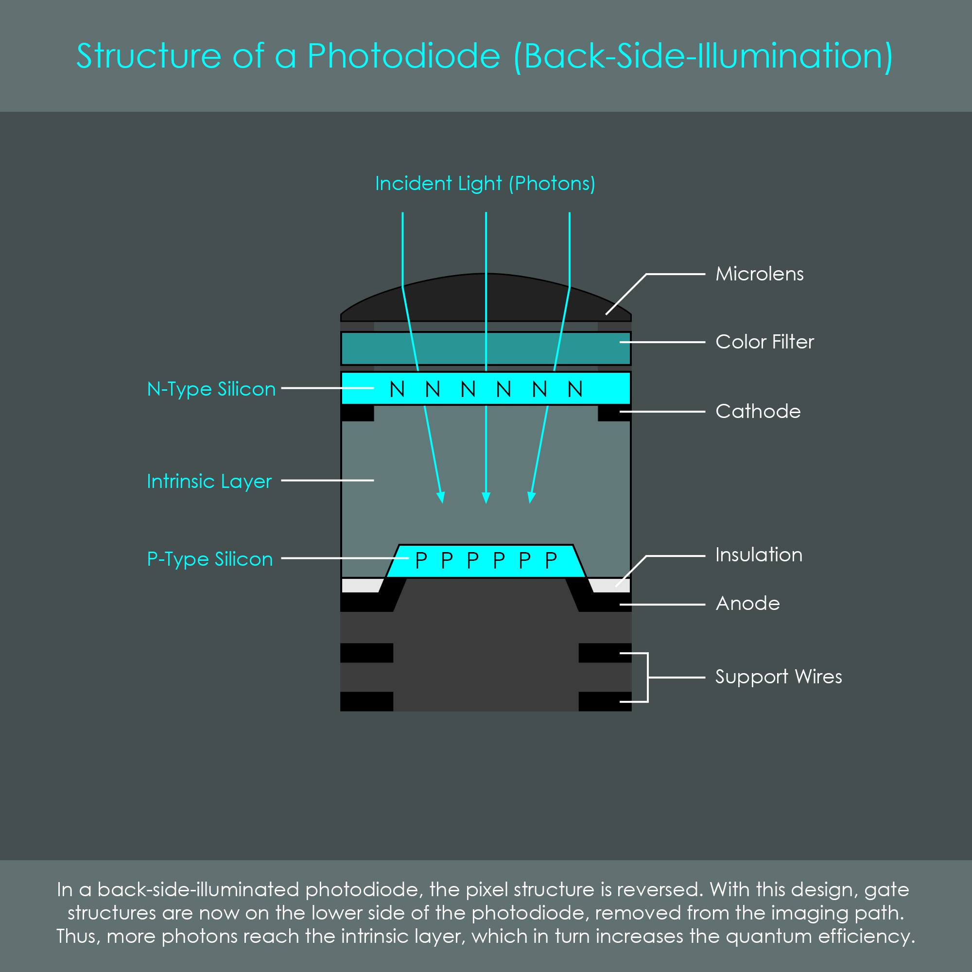
The traditional type of photodiode is designed to collect photons coming from the front side. This is why the traditional photodiode design is also called frontside illuminated. In photodiodes with front side illumination architectures, light must travel through multiple layers of wires and transistors before reaching the actual diode. These layers can block or deflect light from reaching the photodiode reducing performance and causing additional problems such as crosstalk. Crosstalk describes a phenomenon where incident photons are being deflected by metal structures that cause them to accidentally hit a neighboring photodiode. To prevent this from happening, a reflective coating (light tunnel) can be built around the wiring structures so that photons are guided into the intended photodiode. Another way to avoid similar problems and to increase a photodiode’s light sensitivity is to flip the photodiode upside down. By this design, light is collected from the backside of the photodiode with the wires and transistors located underneath. This photodiode design is called backside illuminated and allows light to reach the sensitive area much easier which results in a better quantum efficiency. Please note that backside illumination is just an optional design and not all image sensors are based on this architecture. The figure image shows the principle of a backlit photodiode.
A photodiode only responds to certain wavelengths depending on their semiconductor materials. Their sensitivity can be changed by using different substrates and different dopant materials to modifying their photoelectric properties. In optical communication systems where optical fiber cables are used to transfer light from a sender unit to a sensor, the photodiodes used for signal detection often rely on a binary compound like indium phosphide (InP) due to their higher switching speed. Indium phosphide can be doped in the same way as silicon, the only difference lies in the dopant materials. InP substrate doped with zinc (Zn) results in a p-type InP material, InP substrate doped with sulfur (S) or tin (Sn) results in n-type InP. For the active photon absorption layer, various materials can be used, depending on the wavelengths that need to be detected.
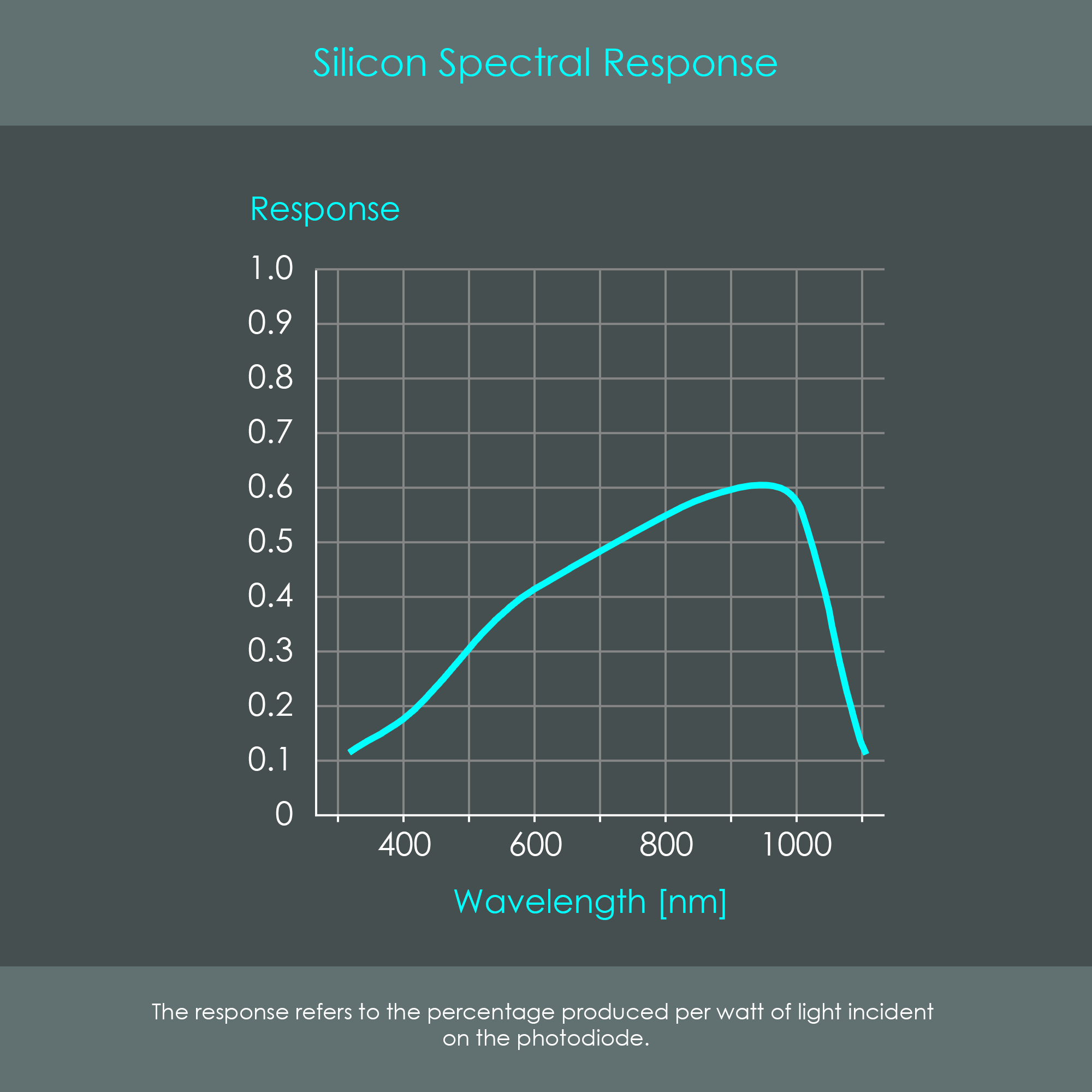
For image sensors in digital cameras, silicon is actually the best choice as it reacts to the visible spectrum of light. Unfortunately, not every photon triggers a reaction in the photodiode. The efficiency can be expressed in the ratio between the generated photocurrent to the incident light power. If every single photon resulted in a current, the ratio would be 100% or 1. In reality, the spectral responsivity for silicon is between 10% and 60% depending on the exact wavelength. The diagram shows the spectral responsivity of a silicon photodiode.
In digital photography, image noise describes an interfering signal similiar to noise in radio technology. Noise becomes noticeable in the form of spots with increased intensity in areas that would normally be illuminated uniformly. Just like noise in audio signals, it is an undesired phenomenon in photography and can degrade image quality significantly. Noise generally affects the entire picture. For a particular pixel, noise adds to the available signal caused by photons and pretends to be light where normally the light intensity would be lower. Even though noise is unavoidable, its relation to the light signal can be so small that noise will not be a disturbing factor. The signal-to-noise-ratio (SNR) is a universal way of comparing the relative amounts of signal and noise. A high SNR will have very little visible noise while a low SNR will show clear noise interferences. There are various reasons for noise to occur and factors that influence the noise performance of a camera sensor. These are the most common types of noise:
This type of noise is always present, even in totally dark surroundings where no photons illuminate the sensor. The reason for dark noise is basically the supply voltage that is necessary to drive the sensor and to allow signal detection. The reverse bias voltage applied to the photodiodes does not perfectly prevent a current from flowing but sometimes allows a tiny ‘phantom current’ to leak at random. Any leaked electrons cannot be distinguished from those excited by light and will also contribute to the readout signal. Also, despite silicon being predominantly responsive for visible light, a photodiode can also be excited by thermal radiation. Thermal radiation simply is the effect of heat and the warmer an image sensor gets, the more dark noise can be produced. Thermal radiation can be available from the surrounding (e.g. using the camera on a sunny day) but can also be induced by the operating circuits (e.g. the reset of a photodiode causes thermal radiation and therefore thermal noise). For typical exposures at daytime, dark noise is typically not observable but it becomes prevalent on night photography where long exposures need to be made.
Fixed pattern noise (FPN) describes a particular noise pattern on digital camera sensors where individual pixels tend to record brighter or darker intensities of light deviating from the general dark noise level. Another difference between FPN and dark noise is that FPN does not occur randomly but is characterized by the same pattern of ‘hot’ (brighter) and ‘cold’ (darker) pixels occurring with images taken under the same illumination. The reasons for the existence of FPN are tiny differences in the individual responsitivity of the photodiodes that might be caused by slight production variations resulting in tiny differences in photodiode size or microlens shape. Again, this type of noise is also more prevalent on pictures taken with longer exposures.
Banding Noise is often caused by sensor readout, downstream amplification, analog-to-digital-conversion and high-frequency components. For this reason, banding noise is also referred to as readout noise or bias noise.
Photon noise, also referred to as Poission noise or shot noise, is a fundamental property of all light sources. A light source typically does not emit photons at a perfectly constant rate but is rather pulsating and emitting photons like raindrops. Also, the timing for new light pulses to occur is not predictable by the observer. The question on how many photons can be expected during a given timespan can only be answered by probability theory. The probability can be calculated by the Poission distribution. Photon noise is independent from other noise sources and constitutes the dominant source of image noise in bright-light situations.
The dynamic range of an image is defined as the ratio of the maximum signal a sensor can record (full-well capacity) and the total noise signal (in the dark), both indicated in electrons. Dynamic range is usually specified by the logarithmic unit dB (decibels). The dB value expresses the factor by which the greatest brightness value is greater than the lowest brightness value. The ratio of two brightness values, l1 and l2, can be converted into a value with the following equation: DR = 20 x lg ( l1 / l2) dB. The dynamic range is an important characteristic of an image sensor as it expresses its ability to record very bright spots and very dark spots at the same time. The maximum signal is given by the saturation of a photodiode.
As described above, the design of the photodiode allows incident light to generate a photocurrent that can be converted to a voltage for read-out. Although there is an almost linear relationship between a photodiode’s exposure to light and the generated photocurrent, there is a threshold that photocurrent cannot exceed regardless of the number of photons hitting the photodiode. The highest possible current defines the saturation of a photodiode. The photocurrent becomes saturated when all photogenerated charge carriers (free electrons and holes) are extracted from the semiconductor. This physical property is the reason why it is often useful to have larger pixels in a camera sensor with more area for an intrinsic layer. Pixels with a very small size (in small sensors or in sensors with very high resolution) often have a very low saturation level. The graph shows the relationship between the number of incident photons and the resulting photocurrent (number of electrons). The saturation point, also known as clipping, is clearly visible at the breaking point of the photocurrent function.
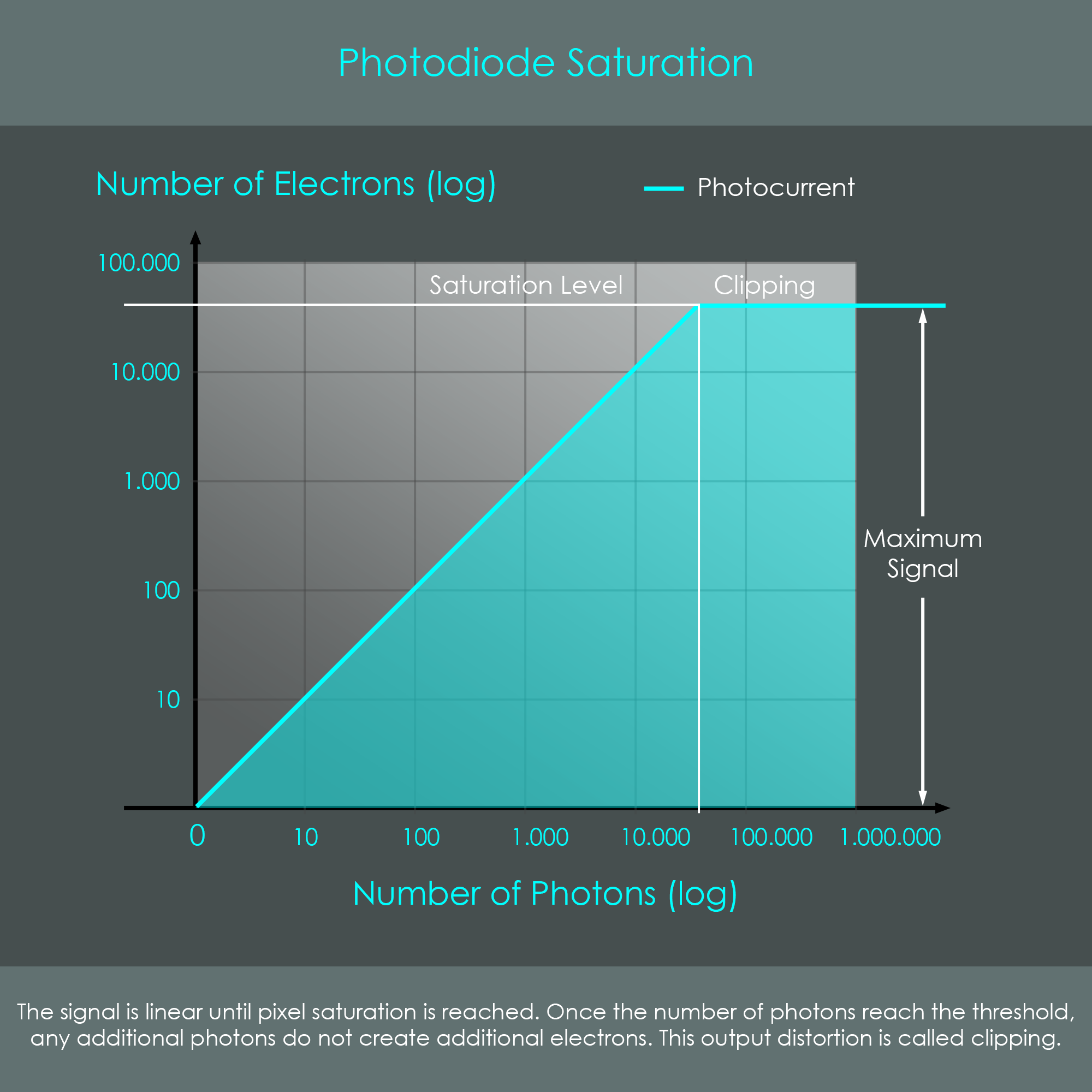
A photodiode that reaches saturation results in a fully white pixel. In addition, a saturated photodiode is not be able to detect any more photons as it is already operating at its limit. There is a high probability for saturated pixels to be actually overflown and therefore they contain less information about the scene than other pixels. For that reason, it is generally recommended for a photo to choose the exposure setting so that the brightest region of interest falls just below the saturation point.
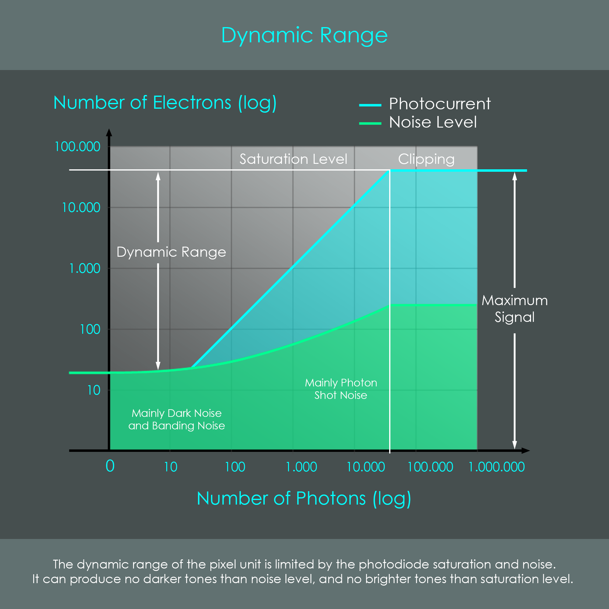
As described, the maximum signal is limited by the photodiode’s saturation level. By contrast, the minimum signal is limited by noise that superimposes low signals so that any lower intensities of light cannot be distinguised from that noise level. The resulting dynamic range of an image sensor is summarized in the diagram.
The challenge in today's photodiode designs is that they are unable to detect the specific wavelength of incoming light, and therefore photodiodes cannot register the color of light. All photons of the visible light spectrum have sufficient energy to let the photodiode react to them by creating an electron-hole-pair. The readout system then measures a current that is established by the electrons flowing towards the n-type side of the photodiode. Electrons however cannot be distinguished from each other as they all have the same energy. Therefore, photodiodes with no additional support structures are not able to detect color and can only create monchrome images, even if the most vibrant colors have illumiated the sensor.
In order to give cameras the ability to recognize the color of light they are capturing, sensor designers are using color filters applied in front of the photodiodes. A color filter is only transparent for certain wavelengths of light while other wavelengths will be absorbed or reflected by the filter. Camera sensors typically have color filters in the base colors red, green and blue. Each color filter provides a certain tolerance so that not only photons of one precise wavelength (such as blue with only 460 nm) will be allowed to pass the filter but an entire range of near-blue wavelengths of light (roughly 400 nm - 490 nm). Photons that have passed the color filter still only produce a current with no color information included. However, the crucial factor is now that the image processor knows which color the photons must have had when exciting the photodiode because the color filters are placed in a fixed pattern. Due to the tolerances of the color filters, the camera's software even recreates all other colors of light that have been in the original scene. You can read more about the color recreation (called demosaicing) in the chapter on signal processing.
A digital camera typically has a number of optical filters applied in front of the actual CMOS sensor. These filters help to block some interfering signals from invisible light or to reduce undesired effects such as moire patterns on subjects.
One disadvantage of low-pass filters, also called anti aliasing filters or blur filters, is that they slightly reduce sharpness. In most cases, that tiny blur is not perceptible, and low pass filters have become a standard solution for the removal of moiré patterns.
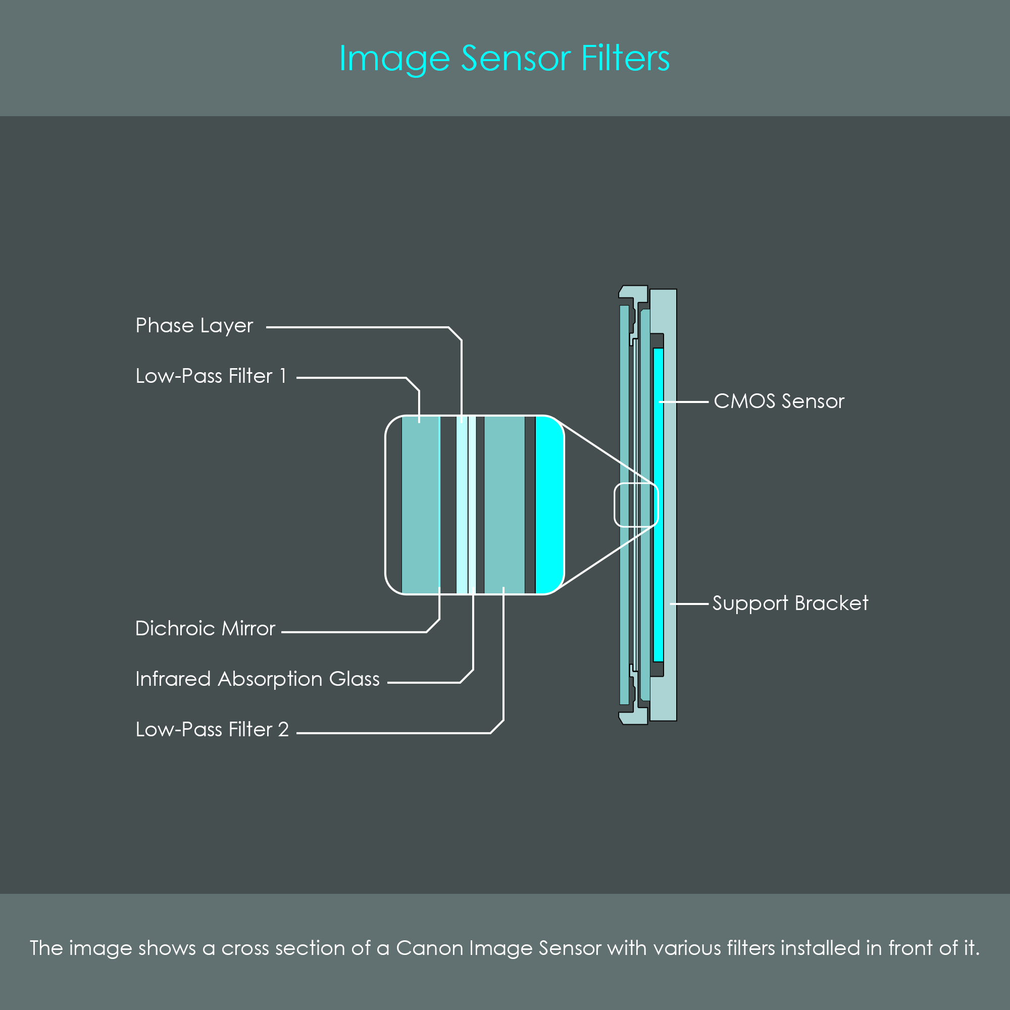
Note that the image does not show the color filters and microlens array that is attached to the actual CMOS sensor. Both of these filters are part of the actual image sensor, and are integrated into the pixel units themselves. However, the color filters add to the total number of optical filters that light has to pass in order to produce an electric signal.