All light coming in through the photographic lens of a DSLR is ultimately captured by an image sensor and is converted into electrical signals. This chapter describes how signals from the sensor are being evaluated and processed.
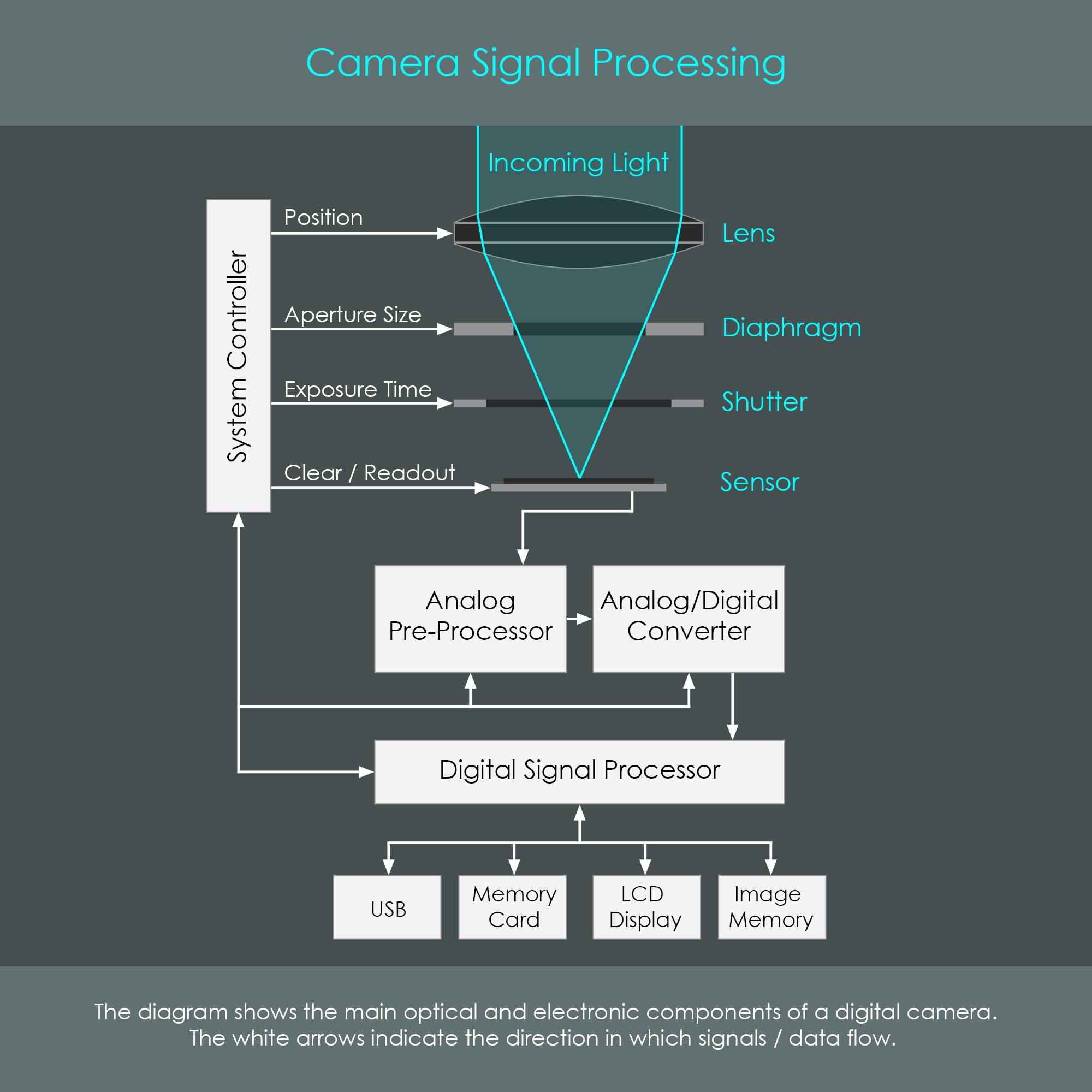
The diagram is an overview of all major components of a digital camera. A system controller does all the adjustments to optical elements but also activates digital post-processing steps. A digital signal processor (DSP) like the Canon DIGIC X processor is the camera's central processing unit, and it is responsible for both image-processing and user interface. Note that this is only a simplified view, and the auxiliary sensors (autofocus, metering), the viewfinder information displays, or the reflex mirror are not shown.
Modern image sensors are highly developed semiconductors with a high level of integration. This means that various driver and post-processing circuits are directly embedded in the image sensor's chip material. A typical 2D image sensor consists of a light sensitive area (the pixel array) as well as an area for the power supply and readout electronics. The architecture of an image sensor allows for each pixel to get addressed individually and to have its signal transported to an analog processing unit where all signals are then transferred to an analog-to-digital converter. The image below shows the drivers and readout units of an image sensor. Each cyan colored square refers to an individual pixel circuit. All pixels are arranged in a rectangular array. The dark background behind pixels represents the substrate material from which the image sensor has been developed, supply lines (supply voltage, ground), row selector lines, and readout lines. The special characteristic of a CMOS sensor is that every pixel unit does not only consist of a photodiode but also has its own readout-circuit included. Some types of CMOS sensors even perform an amplification and charge-to-voltage-conversion still on the pixel.
Once the row selector activates a line (RSL), all pixels from that line apply their charge or voltage (depending on the type of pixel design) to the readout line (RL) that directly leads to the column selector. That column selector is a multiplexer that always connects only one readout line with the analog signal processor. The column selector switches through all columns until all pixels from the selected row have been read out. After that, the row selector activates the next line, and the column readout starts again. Each pixel signal is processed by an analog-to-digital converter, and is forwarded to the digital signal processor unit.

Depending on their readout circuitry, CMOS image sensors can be classified into two categories: Passive Pixel Sensors (PPS) and Active Pixel Sensors (APS).
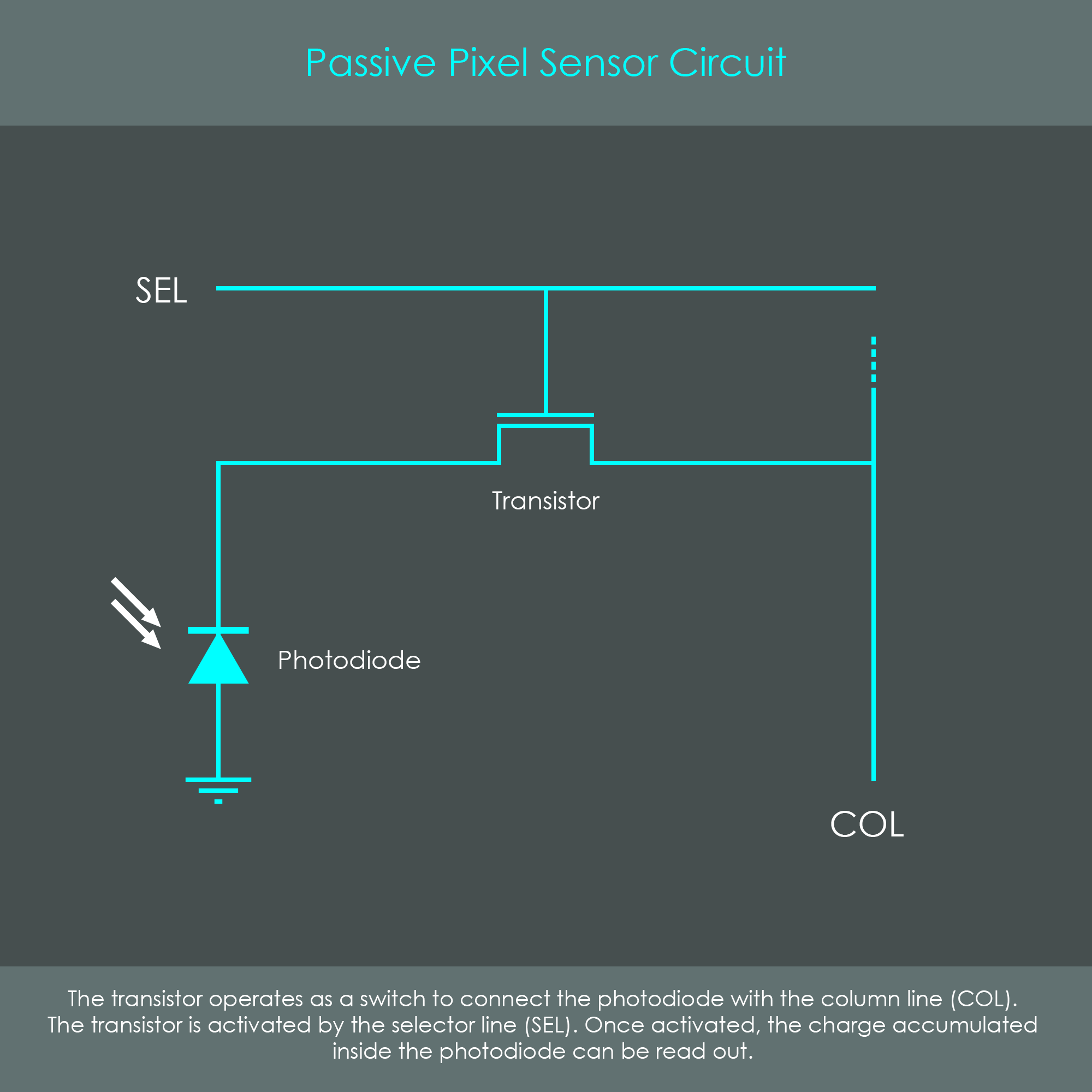
Passive-pixels sensors (PPS) were the first types of CMOS image sensors. When a passive pixel is activated for the light-capturing phase, the photodiode is left floating for a certain amount of time, called integration time. The incident light generates an electric charge across the photodiode. At the end of the integration time, a single readout transistor connects the charged photodiode with a readout line (COL) so that the charge is carried off the pixel. The particular charge of a pixel is amplified and converted into a voltage outside the pixel array, and is then converted to a digital value. This particular setup requires just one transistor which makes the PPS design small and easy to implement. The photodiode can take up more space in relation to readout circuitry and therefore the fill factor of PPS designs is larger than the fill factor of other designs (higher quantum efficiency). On the other hand, the downside of PPS designs is that they are slow to read out, lack scalability and provide a low signal to noise ratio (SNR) resulting in higher noise levels. The diagram shows a typical circuit of a passive pixel unit.
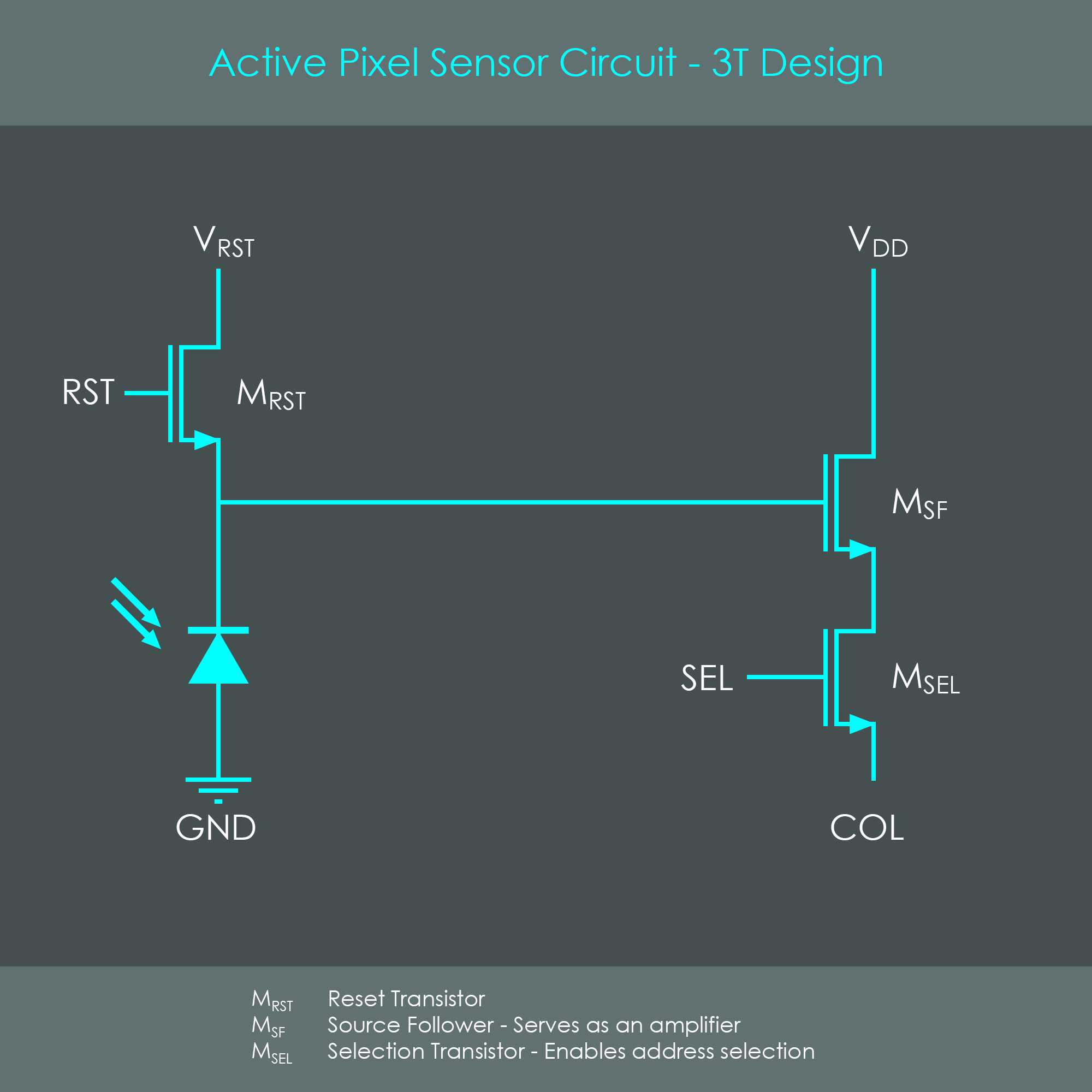
Active-pixel sensors (APS) apply a slightly different approach to convert light into an electric signal. The charge accumulated in the photodiode is read out by sensing the voltage drop across the photodiode with a so-called source-follower transistor. This allows for the photodiode's electric charge to be converted into a voltage still on the pixel. Also, APS designs feature some additional circuitry to perform on-pixel amplification and noise-cancellation. It is this active circuitry that gives the active-pixel device its name. The APS design cancels some issues associated with the PPS design as APS designs are fast to read out and provide a higher signal to noise ratio (SNR) which results in lower noise levels. However, this design has some drawbacks itself. Due to its active and more complex readout circuitry, APS designs usually require three or four transistors, reducing space for the photosensitive area (or alternatively increasing total pixel size) and therefore providing a lower fill factor than PPS designs. It should be noted however that technology has advanced so greatly over the past years that pixel size and fill factor can not longer be considered a real problem. APS designs solve the speed and scalability issues of the PPS design. They generally provide a very economic power consumption and require less specialized manufacturing facilities. CMOS-type APS sensors can combine the functions of image sensing and processing within the same integrated circuit. The diagram shows a typical circuit of a three-transistor (3T) active pixel unit.
The 3T pixel circuit explained:
The 3T pixel light capture process explained:
As the photodiode accumulates charge carriers as long as it is exposed to light, one requirement for 3T APS designs is to have the exposure controlled by a separate mechanical shutter. This would actually not be neccessary if all pixels could be read out at the same time, however in reality the readout process consumes some time so the first line of pixels gets addressed first while the lower lines get addressed later. This type of readout process is called rolling shutter because the activation of the select controllers is done sequentially from the top line to the lowest line in a progressive rolling fashion. Newer image sensor designs have global shutter capabilities, gradually reducing the requirement for mechanical shutters.
An analog-to-digital-converter (ADC) is a circuit implemented within the readout electronics of a camera and it plays an important role in the processing of digital images. Depending on the individual design, sensor pixels either record en electric charge (passive pixel) or have that electric charge converted into a voltage (active pixel). Both electric charge and voltage are analog values. That means that the intensity of analog signals is expressed in an amplitude that can have continuous values. When an image sensor is read out, the readout electronics reads a linear sequence of different amplitudes over a certain amount of time. In order to process and store that image on the camera, computational processing is quired which can only be achieved by digital signals.
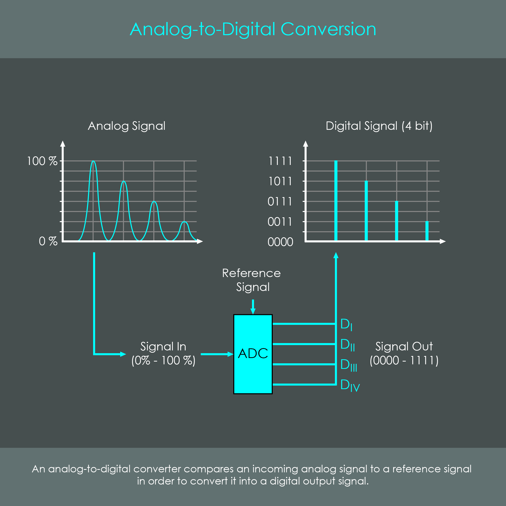
Therefore, an analog-to-digital-converter measures the amplitudes of the analog signals and translates them into discrete values, more precisely into binary numbers that can be used for digital signal processing. For this reason, the ADC is quintessential for the digital image formation as it prepares the signal to be readable by the digital signal processor (DSP) like the Canon DIGIC X processor. The image summarizes the functional principle of an ADC.
Regardless of its internal circuitry, an ADC operates by comparing the input signal to a known reference signal. The digitized output of the ADC is the ratio of the input signal to the reference signal times the full-scale reading of the ADC. One important fact is that an ADC cannot translate every possible amplitude into a binary number. It is rather limited by it’s bitrate that defines how precise the translation can possibly be performed. Therefore, the ADC’s precision can also be compared to a resolution.
It is assumed, for example, that an ADC can only convert analog signals into one bit signals. Such an ADC would classify the analog signals as either pitch black [0] or fully white [1] with no further distinction inbetween. An ADC with a bit depth of two would categorize them into four (2²) groups: pitch black [00], dark grey [01], light grey [10] and fully white [11]. Most consumer digital cameras ADCs with a bit depth of 8, allowing up to 256 (2⁸) distinct values for the brightness of a single pixel. Professional DSLR cameras use 10-12 bit ADCs, allowing up to 4096 (2¹²) distinct values. These cameras typically provide the option to save the 10 or 12 bits of data per pixel in a RAW file because the commonly used JPEG files only include 8 bits of data per channel. The minimum bit rate of an analog-to-digital-converter needs to be based on the sensor’s dynamic range. If the dynamic range of the sensor is for instance 60dB which corresponds to a range of 1000:1, the ADC should provide a bit depth of least 10 bit (2¹⁰ = 1.024 discrete levels) in order to avoid loss of information. Although a 10 bit ADC is a perfect choice in theory and any higher bitrate will not generate additional tonal information, in practice it can make sense to overspecify the ADC to 12 bits to allow for some margin of error on the ADC. It is also useful to have extra bits available to minimize posterization when applying the tonal curve to the linear data. Some camera manufacturers cleverly use this fact to suggest that the digital camera captures images with a bit depth defined by the analog-to-digital-converter. With the explanations above it is easy to understand that this is only true if the image sensor itself has sufficient dynamic range to produce signals with such a high bit depth. The tonal range and dynamic range that a camera outputs can never be larger than the dynamic range of the image sensor.
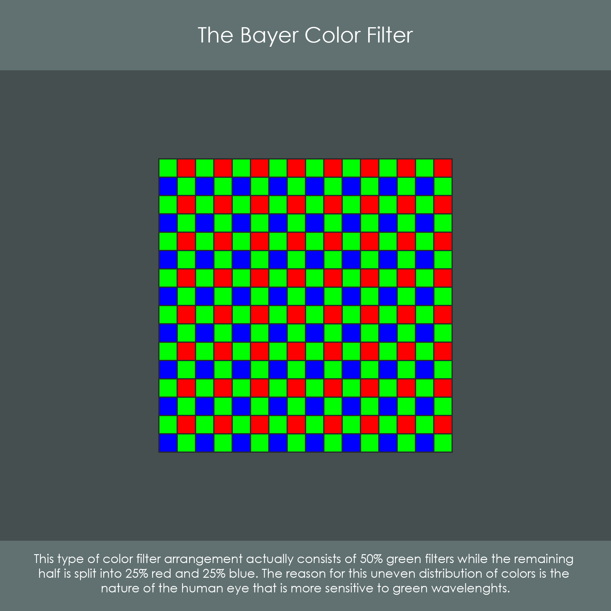
A digital camera sensor typically uses a given arrangement of red, green and blue color filters depending on the type of color filter array (CFA). The most common color filter array used in today’s digital cameras is the Bayer Color Filter as seen on the image. Each square covers one pixel on the image sensor below. This type of color filter arrangement actually consists of 50% green filters while the remaining half is split into 25% red and 25% blue. The reason for this uneven distribution of colors is the nature of the human eye that is more sensitive to green wavelengths. This means that green contributes more to the perception of brightness and contrast than the other colors. The design of the Bayer Color Filter takes this fact into account and helps getting more natural results.
One question is how a color filter array with only three basic colors allows a digital camera to record all possible colors of a photographic scene. Here is how it works: When the sensor actually records light fine color shades are discarded because a photon with aquamarine color (roughly 470 nm) will eventually pass a blue color filter and will therefore simply be registered as a full blue particle of light. However, considering that a photon with aquamarine color has a wavelength that is somewhere inbetween blue and green, such a photon has the same chance to pass a green color filter and get registered as a full green particle. With a million aquamarine photons falling on an image sensor, approximately half of them are going to be registered by green pixels while the other half is going to be registered by blue pixels. The precise wavelength determines the distribution of photons to green and blue pixels. Imagine light with turquise color to be shining on a sensor where the photons wavelength is slightly closer to green (60% green) and slightly further from blue (40% blue). This very distinct color will result in a distribution of electrons with a ratio of 60 (green) to 40 (blue). The same happens to most other colors. Whenever inbound photons have a special wavelength, there will be a specific distribution (for example 70 red to 30 green for orange). The post processing of the image – especially the additive color mixing – will then calculate which precise color shade will result from the single ratios between the base colors. There are exceptions however. Not every color can be described by one wavelenth. Pink color does not have one wavelength but rather is a combination of red and violet light. Only the subjective perception will subliminally add these two different wavelengths to pink color.
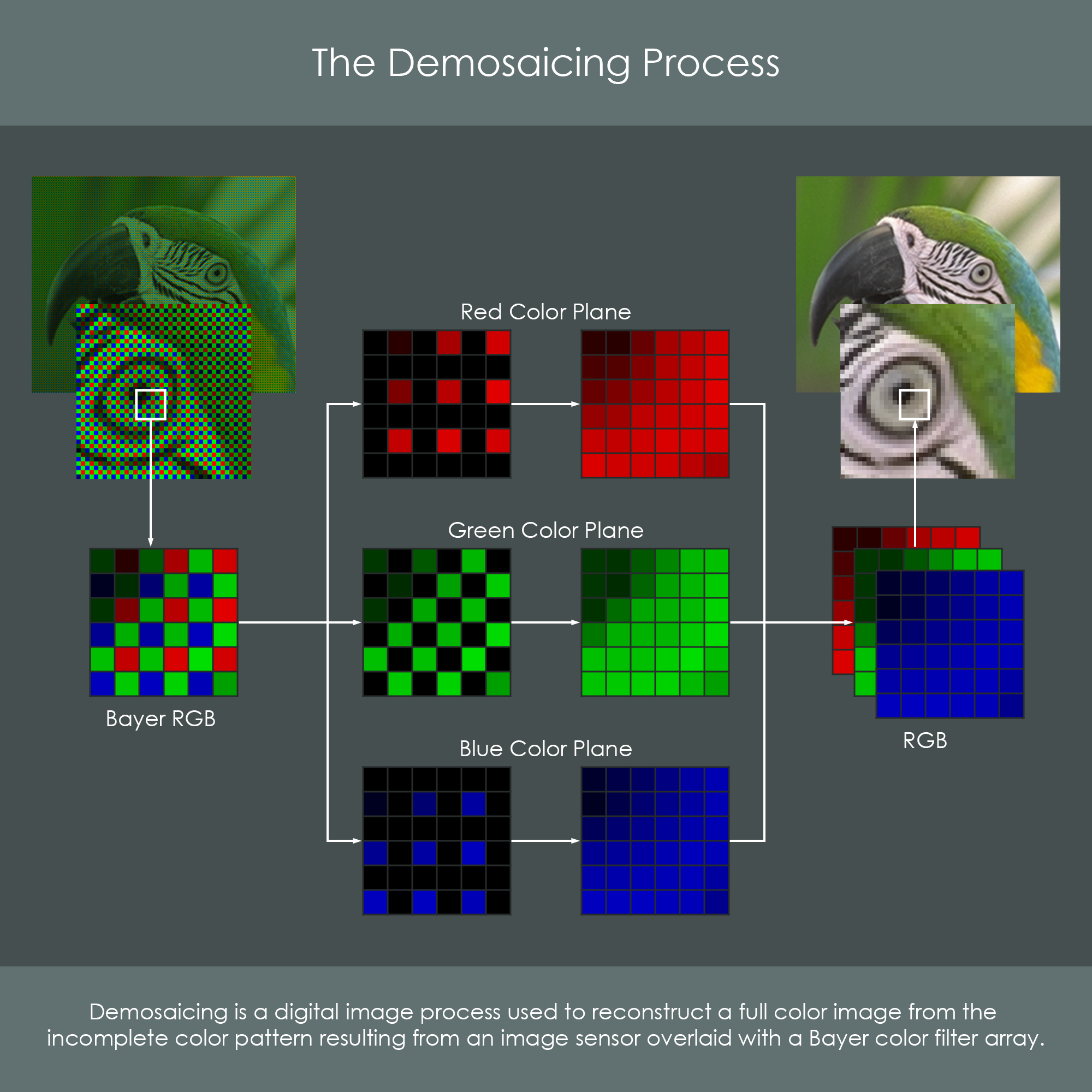
Every color filter array can be separated into its individual layers of color. Looking at one color at a time, each layer has some empty spaces between pixels. Looking at an individual pixel with a green color filter, the resulting signal allows conclusions about the intensity of green light, however there is absolutely no information on whether there was also red or blue light falling onto this pixel and at which intensity. But if you look at the neighboring pixel with a red color filter applied, this time information on the intensity of red light is available, however no information on green and blue light. The blue pixel lacks information on green and red light. The camera’s image processing unit will use this fact to calculate missing color information based on the color intensities of the adjacent pixels. This calculation presumes for a given number of pixels that photons of any color should also have illuminated the pixels inbetween. The image summarizes the entire interpolation process: A small segment of an image sensor's raw image is split into its three color layers. The demosaicing algorithm then determines all missing intensity values and completes the layers. Finally, all three color layers are combined by additive color mixing which produces the final image.
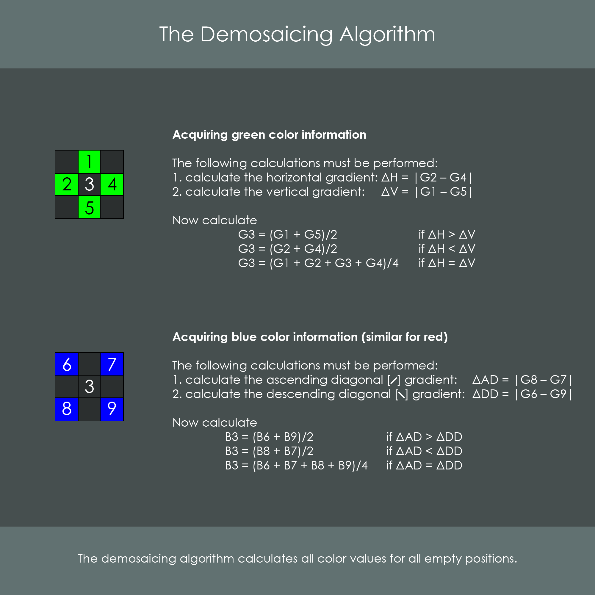
The image shows the calculations performed by the demosaicing algorithm in order to determine the missing values. In the upper case, pixel number 3 is missing green color information. In the lower case, pixel number 3 is missing blue color information. After the calculations, the values can be added to the respective color layers.
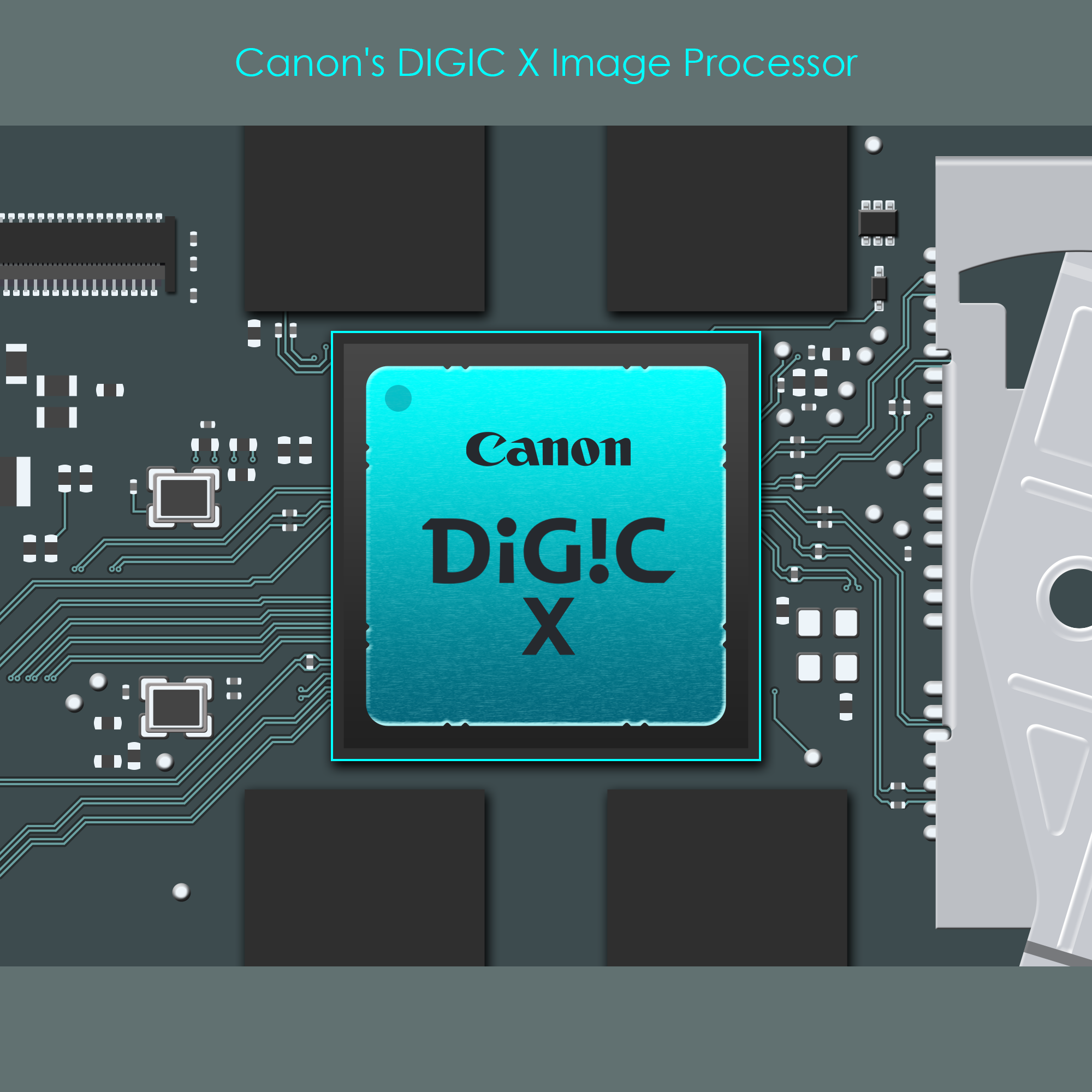
One unit that plays an essential role in the functionality of a digital camera is the digital image processor which is the central signal processing and control unit of the camera system. On Canon EOS cameras, that central processing unit is called DIGIC (Digital Imaging Integrated Circuit). Each version of DIGIC features faster, higher-level data processing capabilities than the previous version. DIGIC is involved in every possible way during the image or video capturing phase.
The DIGIC X image processing engine was introduced in February 2020 with the release of the Canon EOS 1D X Mark III. It is the latest version of the DIGIC platform, and it supports deep learning technology for subject detection, as well as 4k video processing with up to 120 fps.
The list below is a summary of tasks performed by the DIGIC processor. Some of these require substantial image processing power:
If you want to read more about integrated circuits and digital signals, check out this article about microchips.